 2016, Vol. 23


2. Shenzhen Engineering Lab of Flexible Transparent Conductive Films, Shenzhen Key Laboratory of Advanced Materials, School of Materials Science and Engineering, Harbin Institute of Technology, Shenzhen Graduate School, Shenzhen, Guangdong,518055, China
Since graphene nanosheets on atomic scale were obtained by Geim and Novoselov et al. from The University of Manchester, UK, through a micromechanical cleavage method in 2004[1], they have attracted more and more attention of researchers and scholars at all levels worldwide[2-5] owing to their outstanding properties, novel functionalities, low raw materials cost, and versatile applicability. In the last decade, as a star material, graphene, i. e. , atom-thick graphite, has been listed on top materials among numerous new materials and becomes a rising star in the fields of materials, chemical, physical, energy, and environmental sciences and medical diagnosis accompanying with an unprecedented research upsurge. Papers and reviews about graphene would receive priority right of publication. Single-layer two-dimensional graphene would be a universal building block of carbon-based materials and could be a parent of all other dimensions of carbon nanomaterials with diversity morphology. It can be carefully curved to form zero-dimensional buckyballs and many other non-tubular fullerenes and one-dimensional carbon nanotubes. The transportation and movements of electrons and holes through the two-dimensional graphene are quite different from those of common three-dimensional graphite. Both the excellent crystal quality and electronic properties of graphene endow with an extraordinary performance that is difficult to be achieved by common materials[6]. For example, a completely exfoliated and isolated graphene sheet, i. e. , an individual graphene sheet, has a large theoretical specific surface area of 2 630 m2/g (but the best graphene samples produced by industry have practical specific surface area between 1 000 and 1 800 m2/g, even those that are characterized by TEM as being single layer), thermal conductivity of 5 300 W/(m·K) that is higher than carbon nanotube and diamond, high mechanical modulus of 1 060 GPa, high electronic mobility of 15 000-60 000 cm2/(V·s) at ambient temperature, optical transmittance of 97. 7%, extremely high electrical conductivity of 106 S/cm(the highest value among all kinds of materials), perfect quantum tunnel effect, and very anomalous quantum hall effect[1]. Graphene membrane with micrometer size has sufficient stiffness so that it will not be scrolled or folded like common flexible fabrics but has extremely large loads capacity of millions of times exceeding its own weight[7]. Graphene derivatives modified by a variety of molecules or functional groups have opportunities to develop new functionalities[8]. These unique properties make graphene an almost omnipotent material, having broad application prospects in solar cells[8-9], light-emitting diodes[10], alternatives for ITO and FTO transparent electrodes[10-11], liquid crystal displays[12], large-scale pattern stretchable electrodes[13], electrode materials of lithium ion batteries[14], electrochemical supercapacitors[15-16], field effect transistors[17], memory devices[18-20], sensors[21-22], electrochemical biosensor[23], anticorrosive coatings[24], hydrogen storage materials[25], highly active biomimetic oxidation catalyst[26], methanol fuel cell catalyst[27], and a variety of composite materials[28-29]. Especially, field effect transistors made of graphene are expected to replace the current popular silicon transistors in high frequency circuit, which would make it infinitely broad for high frequency boost of supercomputers and other electronic equipment. Also, graphene can be used in terahertz spectral region that gets little development in the whole electromagnetic spectrum, which is connected with the tunable forbidden band width of graphene. The forbidden band width of graphene can be designed into range of 0-3 eV by tailoring it into micro or nano wide ribbons[30], just covering a terahertz frequency range of 1-10 THz[31]. The adjustable band gap makes graphene have the potential to be applied in terahertz emitter and detector. This multifunctional graphene is expected to become a new super material following carbon nanotubes[32] and high aromatic organic materials with high thermal stability, such as conductive polymers[33-34], conjugated polymers[35], and so on. It was reported that the melting temperature of graphene is 4 510 K, about 250 K higher than that of graphite using the same interatomic interaction model[3-6], strongly suggesting that graphene is the most refractory of all known materials. The 2D elastic modulus of graphene could be enhanced to be up to 700 N/m by controlled defect creation[37]. The extraordinary strength, stiffness and lightness of graphene have generated great expectations of its application in flexible electronics and as a mechanical reinforcement agent. The structure and main properties of graphene-based nanomaterials have been summarized in Table 1[4, 38-45].
| Table 1 Overview of structure and main properties of graphene-based nanomaterials |
2 Strategies for Synthesis of Graphene
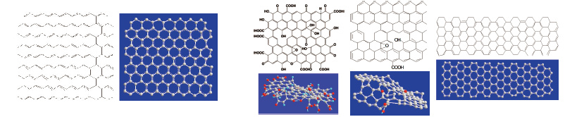
Such an amazing graphene has steep demands for the chemical structure of itself. High quality or perfect molecular structure of graphene is guarantee of its performance because any defects that are not allowed will greatly damage the material performance. Therefore, the preparation of graphene is quite critical. At present, the preparation of graphene focuses around two routes that could be further classified into seven typical preparation methods summarized in Table 1, one of which is the “top-down” micro processing method, and the other one is the “bottom-up” chemical synthesis method[46]. The corresponding target products are also split into two broad areas: large-area defect-free 2D graphene nanosheets with zero band gap and zigzag or armchair edges-containing quasi-one-dimensional graphene nanoribbons with a certain band width and infinite length. For graphene nanosheets, it is expected that their area is large enough so that their excellent properties can be maximized to some extent. And for graphene nanoribbons, their band width is expected about 10 nm or below, so that the tailored graphene shows finite lateral size and electrons will be limited on the lateral direction, which will open up the energy gap of graphene, realizing the switching characteristics of field effect transistors. Apparently, it is more suitable to use the “bottom-up” chemical synthesis method for preparation of atomic scale graphene nanoribbons.
2.1 Synthesis of Graphene Nanoribbons by Polycondensation of Polycyclic AromaticsAs mentioned above, graphene, the thinnest two-dimensional material in nature, has abundant outstanding properties and functionalities. Laterally confined, thin, and long strips of graphene, namely, graphene nanoribbons (GNRs), as novel materials, demonstrate amazing properties distinct from those of other carbon allotropes. The all-semiconducting sub-10-nm graphene ribbons can bypass the problem of the extreme chirality dependence of the electrical conducting nature of carbon nanotubes in future electronics[47]. GNRs have great potential to replace silicon in future electronics and find indispensible application in new energy and materials fields. Thin graphene ribbons containing straight edges gradually transform from semiconductors to semimetals as their width increases[47]. It is difficult to obtain graphene nanoribbons with smooth edges and controllable widths at high preparation yields. Therefore, great efforts have been devoted to productively achieving high-quality GNRs with narrow widths and smooth edges[8]. Chemically synthetic, lithographic, and sonochemical procedures are known to produce microscopic samples of graphene nanoribbons[47]. In other words, there are three representative methods of preparing GNRs—the direct synthesis of GNRs by polycondensation of polycyclic aromatics, unzipping of carbon nanotubes (CNTs), and cutting of graphene nanosheets.
Müllen group and Hanke group have got fruitful research achievements in the syntheses of graphene nanoribbons. They chose Au (111) or Ag (111) surfaces as the substrate materials, 10, 10'-dibromo-9, 9'-bianthryl as precursor monomers. Then the monomers are deposited onto the solid substrate surfaces by thermal sublimation and heated the substrates to 200, 300 and 400 ℃ periodically, inducing the dehalogenated radical addition reactions, intramolecular cyclodehydrogenation and full cyclodehydrogenation polycondensation of the precursor, respectively, and forming graphene nanoribbons eventually[49-51]. The graphene nanoribbons made by this atomic self-assembling reaction showing armchair edges and band width of only 2 nm are the narrowest 1D graphene nanoribbons so far and have widespread potential to become the high performance heterojunction for producing nanoscale electronic devices. Negri et al. reported the copper-mediated trimerization of perylene bisimides along bay regions to construct graphene nanoribbons that are functionalized by arrays of imide groups[52]. Considering that some heteroatoms and structure defects in the GNRs synthesized by this method are unavoidable, it seems that the properties of the GNRs are not as good as those by unzipping carbon nanotubes.
2.2 Preparation of Graphene Nanoribbons by Unzipping Carbon NanotubesTour et al. prepared a nearly 100% yield of graphene nanoribbon structures by lengthwise cutting and unraveling of multiwalled carbon nanotube (MWCNT) side walls via a simple solution-based oxidative and reductive reaction[47]. Ribbon structures obtained thus have high water solubility and can be reduced to graphene nanoribbons in restoration of electrical conductivity. Dai et al. showed an approach to making GNRs by unzipping MWCNTs through plasma etching of the nanotubes partly embedded in a polymer film[53]. Importantly, the GNRs achieved thus have smooth edges, narrow width distribution (10-20 nm), and high quality. This method can be further used to transform few-walled CNTs into sub-10-nm GNRs with band gaps sufficient for fabricating room-temperature transistor. Unzipping CNTs with well-defined structures in an array will result in the formation of GNRs with controlled widths, edge structures, placement and alignment in a scalable fashion for device integration.
Furthermore, the optimization of the GNR properties through modifying the nanoribbon width and edge structure would widen the applications of GNRs in electronic devices. It is reported that self-assembly of sulphur-terminated graphene nanoribbons from a random mixture of molecular precursors within a single-walled carbon nanotube can ensure propagation of the nanoribbon in one dimension and determine its width[54]. It is revealed that elliptical distortion of the nanotube can result in helical twist and screw-like motion of the nanoribbons obtained, suggesting novel ways of controlling the properties of these nanomaterials, including the electronic band gap and the concentration of charge carriers. These nanoribbons can eventually realize vital applications in fields of electronics and composite materials where bulk quantities of nanoribbons are required[55-56].
Besides, chemical vapor deposition is also an important process to successfully produce macroscopic quantities (grams per day) of long and highly crystalline graphene ribbons (<20-30 μm in length) graphene nanoribbons with widths of 20-300 nm and small thicknesses (2-40 layers) using ferrocene and thiophene as raw materials at 950 °C[57]. These graphene layers usually exhibit perfect ABAB. . . stacking as in graphite crystals. Note that the chemical vapor deposition is an even more powerful technique of synthesizing graphene nanosheets, as described below.
2.3 Synthesis of Graphene Nanosheets by Chemical Vapor Deposition of HydrocarbonsAs for graphene nanosheets, their synthesis seems more difficult because of their large size on 2D plane. A cruel fact is that whatever type of preparation methods used will all make the obtained graphene that should have a standard hexagonal structure lose carbon atoms, leaving the production of graphene with defect structures. In order to apply this type of graphene on a large scale, two problems must be firstly solved: producing graphene with a large area and guaranteeing its perfect structure. However, there is no method truly meeting the requirements till today. This is also the root cause why there is no method dominating the field of graphene synthesis so far. How to efficiently, scalably, and controllably prepare large area and high quality graphene nanosheets is a challenging and important research subject in graphene field at present.
For the unsolved difficulties in the preparation of 2D graphene, researchers have explored several ways. Among these methods that can be used to obtain large area graphene, the typical methods including crystal epitaxial growth method on silicon carbide (SiC) with high vacuum annealing treatment[58], chemical vapor deposition (CVD) method with methane as carbon sources and mixtures of hydrogen and argon as dilute gas[59-61], low-temperature inductive coupling CVD[62], and low-temperature microwave plasma CVD[63], have be used to successfully grow large-area graphene with diameter more than 1 cm and the CVD method is also compatible with the existing semiconductor production technologies. Recently, a reusable germanium substrate was reported[64]. After covering silicon wafer surface with a hydrogen-terminated germanium buffer layer, its anisotropic nature allowed multiple nucleated graphene crystals to grow along the same orientation, which could make single seeds connect each other easily, successfully realizing the production of single-crystal monolayer graphene with large size. And the obtained graphene could be easily transferred to other substrates without etching the germanium substrate. Specially, a laser-induced graphene growth method was found to directly synthesize graphene by a focused laser irradiation[65]. A photosensitive resin film with a thickness of 30 nm was coated on quartz by spin-coating, and then this coated quartz wafer was covered by another piece of transparent quartz wafer. Next, a continuous wave Nd:YAG laser irradiation with a power of 2. 8 W and wavelength of 532 nm was focused on the coating film for 3-5 min. The carbon atoms were decomposed from the photosensitive resin, then dissolved in the molten quartz, and extracted to form graphene when the temperature of quartz was decreased. Importantly, this method did not need metal catalysts and the formed primary 2-3 layer graphene showed a sheet resistance of 780-805 Ω/sq, which had great potential in the assembly and application of electronic devices.
Usachov et al. discovered perfect structural properties and simultaneously highly spin-polarized charge carriers of a single graphene layer grown by chemical vapor deposition of propylene at 10-6 mbar and 660 ℃ for 15 min on a layer of Co(0001)[66] . A highly ordered graphene perfectly oriented with respect to the substrate has been observed by low energy electron diffraction (LEED) and scanning tunneling microscopy (STM). As seen in Fig. 1(b),(d), the carbon atoms, packed into the graphene matrix, perfectly fit the lattice of the underlying cobalt layer. The graphene prepared at 560 °C is characterized in LEED by the arc-shaped reflexes (Fig. 1(a)), which is consistent with STM observation (Fig. 1(c)), implying the presence of predominant misoriented domains. Stride et al. reported gram-scale production of a fused array of graphene sheets at a final yield of 0. 1 g per 1 mL of ethanol—typically yielding ~0. 5 g per solvothermal reaction dispersed by mild sonication of non-graphitic precursors in a bottom-up approach[67].

|
Figure 1
Graphene structure in real and reciprocal space. LEED patterns of graphene/Co(0001) for (a) misoriented graphene domains and (b) perfectly oriented graphene synthesized at 560 and 660 ℃, respectively. STM images for (c) misoriented domain, rotated by~10° relative to Co(0001) lattice and (d) graphene aligned in a registry with the substrate. The horizontal direction is parallel to the  |
Quite recently, Huang et al. successfully constructed a novel 3D architecture from a tubular graphene network foam (Fig. 2(a),(b) ) with hollow, trihedral, tetrahedral and pentahedral joints (Fig. 2(c),(d)) by template directed CVD technique and subsequent annealing process[68]. Tubular graphene was grown at 1 100 ℃ by CVD onto a SiO2 monolith template in a gas flow of CH4, H2, and Ar. As shown in Fig. 2(a),(c),(d) the 3D graphene has a topologically identical tetrahedral skeleton and looks like amorphous silicon. The 2D band shift characteristic of few-layer graphene and a very small intensity ratio of D to G bands (ID/IG = 0. 13) of its Raman spectra (Fig. 2(e)) show that the tubular graphene has high-quality without defects. Fig. 2(f) shows that the 3D graphene has misoriented polycrystalline nature with a sharp (002) diffraction corresponding to an interlayer distance of 0. 342 nm. It is interesting to find that the 3D graphene architecture exhibits a continuous, graphitic, hydrophobic, 99. 9% porous, indestructible (by fire and chemicals), feather-light with a ultralow density down to 1. 6 mg/cm3, bulk material with metal-like conductivity up to 80 S/cm, a specific area of nanopowder, unprecedented strength and modulus up to 100 MPa, full shape memory after 95% compression and unbelievable robustness (over 80% maximum stress retention after 1 000 cycles of 80%-90% compression). The >99. 9% porous tubular graphene has a wall thickness of 1. 0 nm corresponding to 2-3 graphene layers and a large specific surface area up to 970 m2/g, while the graphite powder has specific surface area of only about 8. 5 m2/g. The multifunctional material having ultralight, ultrastiff, and ultrastrong features would be applicable in energy, catalysis, and thermal/electromagnetic shield.

|
Figure 2 (a)-(d) SEM images of 3D graphene and hollow graphene tubes. (e) Raman spectra of 3D graphene, graphite, and RGO sheet containing 10 % oxygen. (f) Selected area electron diffraction pattern of a graphene tube from TEM[68] |
2.4 Preparation of Graphene Nanosheets by Reduction of Graphene Oxides from Graphites
The most valued preparation method is the laser scribing strategy[69-70], which selectively reduces GO to graphene with a specific surface area of around 1 520 m2/g (compared with 1 000 to 2 000 m2/g for a typical activated carbon material) by focused light scribing of GO film that is drop-cast onto a flexible polymer film substrate with a 788 nm infrared laser using a commercially available CD/DVD optical drive. The reduction degree of GO can be quantitatively controlled by adjusting the time of laser focusing. After selective laser scribing, reduced and unreduced GO areas can be formed. Such laser scribed film can be also simply transferred to other substrates to build flexible electrodes for device assembly. Laser scribed graphene is expected to be better than the expensive carbon nanotubes on manufacturing cost and performance. At the same time, flexible patterning electrode constructed with highly reduced laser scribed graphene could also realize the detection of 20 ppm of NO2 in air[70]. So far as dry reduction of GO was concerned, camera flash could remove the oxygen of GO to obtain graphene and the use of freeze drying GO foam block could further enhance the deoxidation result[71]. Although the dry process can avoid the agglomeration problem that exists in wet process and realize the scale production with the use of optical drive or flash, certain problems still exist in their laser-irradiated areas.
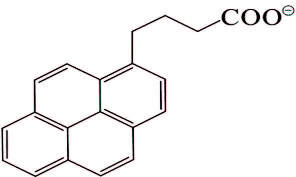
Undoubtedly, chemical method is the main way for large-scale preparation of graphene. Among the strategies of “bottom-up” chemical synthesis of graphene, chemical synthesis with benzene and polycyclic all-benzenoid aromatic hydrocarbons as the starting materials is one of the typical methods for production of 2D graphene molecules. Currently, the most commonly used all-benzenoid aromatic hydrocarbon is hexa-peri-hexabenzocoronene (HBC), also known as “super benzene”. With good properties, HBC contains huge potential applicability, inducing the current research upsurge of HBC and the formation of a new research field—“super benzene” chemistry. And graphene molecules with huge plane can be prepared by dehydrogenation of HBC's branched derivatives with catalysis of FeCl3 or Cu(OTf)2-AlCl3[72]. Soft-landing solvent-free matrix-assisted laser desorption/ionization mass spectrometry of solid state HBC is another route to obtain ultrapure crystalline architectures of giant graphene molecules[73]. In this case, the nanographenes are transferred to gas phase, purified and adsorbed or soft deposited on a proper surface. The STM clearly demonstrated highly ordered nanoscale suprastructures of the graphene molecules. However, complicated characteristics especially rigorous reaction conditions of the synthetic method could lead to the rearrangement and isomerization of carbon atoms during synthesis process that may bring structure defects.
2.4.1 Preparation of graphene nanosheets by oxidation and reduction of graphiteConsidering the high cost of graphene synthesis, the "top-down" method for preparing graphene with much cheaper graphite as the starting material is more favorable to large scale-production of graphene nanosheets. The most common method is the GO reduction method. After oxidizing graphite through modified Hummers method[74-75], the generated oxygen-containing groups such as carboxyl, hydroxyl, and so on, can increase the interplanar spacing and promote loose structure of graphite and then stably dispersed GO hydrosol can be obtained ultrasonically. Then, this disassembled graphene is stabilized with all kinds of stabilizers. Finally, graphene nanosheets are formed after removing the oxygen-containing groups of GO by chemical reduction of hydrazine or sodium borohydride. Among the “oxidation-stabilization-reduction” trilogy, the head one and end one are all classic and show little variables. The main variables exist in the second part “stabilization”. For GO whose surface conjugated π bonds have been destroyed, plentiful oxygen-containing groups covalently bonded on the surface of GO can make it get steady dispersion temporarily. However, once these groups are removed, their stabilizing effect disappears immediately. Therefore, the stabilization steps of GO determine the exfoliation efficiency of the finally resulting graphene and the yield of single-layer (i. e. monolayer) or few-layer (i. e. 2 to 10 layers) graphene.
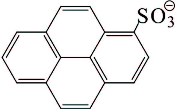
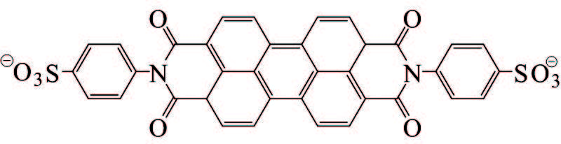
1) Stabilization of GO by external stabilizers. It seems that dispersing stabilizers are necessary to realize a stable dispersion of hydrophobic graphene nanosheets in water. Effectively stabilizing GO through covalent or noncovalent bond interaction by π-π interactions with GO sheets is the main ways to obtain steadily dispersed reduced graphene. The investigation on covalent attachment of some compounds to decorate and stabilize GO involves introducing benzenesulfonic acid via sulfonation reaction[76], poly(vinyl alcohol) via esterification[77-78], polystyrene via esterification and nitroxide radical coupling reaction[79], isocyanates via amination and esterification reaction[80], and functionalizing GO with styrene-b-ethylene-co-butylene-b-styrene triblock copolymers via click chemistry[81]. There is no space to discuss them in depth here, but we concentrate on discussion about stabilization of GO by noncovalent π-π interactions stabilization. The mainly involved stabilizers are aromatic macromolecule compounds and macromolecular polymer stabilizers that are all attached firmly on the graphene surface through π-π stack and hydrophobic effect to reach the purpose of preventing graphene nanosheets from agglomeration and precipitation. In addition to the pure fused-ring aromatic hydrocarbons 3, 4, 9, 10-perylene tetracarboxylic acid[82-83] and 3, 4, 9, 10-perylenetetracarboxylic dianhydride[84], pyrene or naphthalene-like polycyclic aromatic derivatives containing 3 or 4 rings, such as 1-pyrenebutyrate[85], pyrene-1-sulfonic acid sodium salt (PyS)[86], disodium salt of 3, 4, 9, 10-perylenetetracarboxylic diimide bisbenzenesulfonic acid[86], methylene green[87], and so on, are commonly used (Table 2) and also show good effects. The most striking feature is that these organic compounds are water soluble due to the presence of carboxyl and sulfonic acid groups, quaternary ammonium ions or N, N-dimethyl on them, and therefore black or carmine graphene aqueous dispersion in a concentration range of 0. 1-0. 15 mg/mL could facilely be obtained after the reduction with hydrazine. Although the contents of graphene in these aqueous systems were not very high, vacuum filtration of these dispersions could produce free-standing flexible graphene film with a thickness of several micrometers. And the film showed a conductivity of 2 S/cm, almost seven orders of magnitude higher than that of GO, and could be used as an electrocatalytic layer for modifying the FTO counter electrode of a dye-sensitized TiO2 solar cell[86]. Moreover, the conductivity of graphene film stabilized with PyS was dramatically increased up to >1 100 S/cm after thermal treatment of the film, which could be attributed to further reduction of GO. And the optical transmittance of the graphene film directly deposited on quartz substrate with a thickness of only 10 nm is excellent enough to replace ITO as the anode materials of solar cells[86].
| Table 2 Noncovalent stabilization of graphene in aqueous medium by water soluble large aromatic molecules |
Tetrapotassium of coronene tetracarboxylic acid (CS) with a larger π planar (Table 2) was useful to stabilize thermal exfoliation of graphite oxide ((5±1) layers)[88-90] and graphene ((3±1) layers) prepared via arc discharge method in hydrogen atmosphere[91]. With 4 carboxylic acid groups, CS was highly soluble in water. Also, CS showed a blue fluorescence and also liquid crystallinity at the same time. It must be pointed out that coronene was electron enriched, but the carboxylates of CS were known to be electron deficient. Exactly, utilizing the electron deficiency of CS containing large aromatic planar could realize stabilization of graphene by strong interaction with the surface of graphene sheets through synergistic noncovalent charge-transfer and π-π-stacking interactions.
In fact, noncovalent modifying and stabilizing agents based on organic compounds are not only used in graphene dispersions, but also in graphene films. Noncovalent functionalization of graphene with self-assembled pyrene buanoic acid succidymidyl ester[11] followed with light irradiation reduction could promote the wettability of graphene. And the resulted graphene films with few layers through this noncovalent modified CVD method could be used in organic photovoltaic battery anode to significantly improve the battery performance.
Macromolecular polymers used for noncovalent stabilization of graphene include high molecular weight poly(sodium 4-styrenesulfonate), polystyrene, poly(vinyl alcohol), conductive polymer sulfonated polyaniline, and so on. For example, the resulted black aqueous dispersion of GO coated by poly(sodium 4-styrenesulfonate) with a weight-average molecular weight of 70 000 at a concentration of 0. 1 mg/mL can remain stable over a year[92]. When the content of reduced graphene stabilized with sulfonated polyaniline in the aqueous solution was higher than 1 mg/mL, the formed composite film by a filtration method of the dispersion showed a conductivity of 0. 3 S/cm[93]. It must be noted that the molecular weight of polymer is one of the key factors affecting the stability. Only those polymers with appropriate molecular weight can strongly and stably disperse GO and graphene[94].
Sometimes, partially prereduced GO as stabilizers can also efficiently stabilize graphene. After adding organic solution of functional groups-terminated polymers to the aqueous dispersion of partially reduced GO, because the carboxyl groups remained on the reduced GO provide complexation sites to the protonated amine-terminated polymers, this noncovalent interaction would transfer the reduced GO to the organic phase, resulting in stable dispersion of the reduced GO in the presence of polymer stabilizers[95].
2) Stabilization of GO by its own electrostatic repulsion. It could be more valuable to realize stable dispersion of graphite or graphene in water through the electrostatic repulsion in the absence of any dispersant or polymer stabilizers[96-97]. Once ammonia was added to GO aqueous solution to increase the pH to around 10 and then the GO solution was reduced with hydrazine, a high-performance graphene with a conductivity of 72 S/cm, a tensile modulus of 35 GPa and an optical transmittance of >96% would be accomplished and afterwards converted onto flexible paper. Alkaline environment with a pH of 10 could convert the carboxylic groups on GO surface to carboxylic acid anions, resulting in a strong electrostatic repulsion between graphene nanosheets, which realized the stable existence of graphene. And it has been reported recently that GO under faintly acidic condition with thiosemicarbazide as reductant in the absence of special stabilizer could be also used to produce graphene nanosheets with a thickness of 0. 64 nm[98]. Although preparation of GO-based graphene is one of the main methods for graphene production on a large scale, this method still faces many challenges, for example, the obtained graphene contains impurity and many heteroatoms after the oxidation process, the stability problem of GO-based graphene at a higher content is more difficult to thoroughly resolve, and high toxicity, strong corrosivity and air sensitivity of typical reductants including hydrazine, hydroquinone, and dimethylhydrazine used commonly make the graphene preparation even harder.
All the graphene obtained by these chemical methods actually exists as dispersions of graphene. Besides, there are also reports on the preparation of powder state of graphene nanosheets. Freeze drying graphene derived from in situ reduction of GO dispersion could produce solvent-free and organically dispersible graphene nanosheets[99]. Not only could this dried graphene powders be stored and transported easily, but also could be well redispersed in solvents. Graphene nanosheets with a thickness of 0. 57 nm were obtained from the dispersible graphene in DMF at content of graphene of 0. 2 mg/mL. Obviously, this freeze drying method without using any solvent is an environmentally friendly green method.
2.5 Preparation of Graphene Nanosheets by Direct Exfoliation of Graphite without OxidationReduced GO has been recognized as a non-feasible alternative to defect-free graphene, and attention is turning towards reliable methods for the high-throughput direct exfoliation of graphite. A way to fundamentally solve the above problem is to avoid GO and directly utilize graphite without oxidation process. This way can fundamentally guarantee in which intrinsic carbon element in graphene sheets will not be hybridized and then the intrinsic structure of graphene sheets will not be damaged. In the obtained graphene by this way, there are no heteroatoms such as oxygen or electron-withdrawing groups including —COOH and CO that could usually be found in reduced GO. As a result, this method can well reserve intrinsic structure and functions of graphene to a great degree. Obviously, the resulted graphene by this method has higher quality than the products of the method with GO as intermediate.
Synthesis of graphene nanosheets on a large scale is urgently required for its wide application and further commercialization. Several classic routes have been proposed to prepare graphene nanosheets, including micromechanical cleavage of graphite using Scotch tape[1], and liquid-phase exfoliation of graphite by using sonication and supercritical fluid[100]. Among them, the Scotch tape method as the simplest original one can create the best graphene nanosheet samples with a seriously limited yield of graphene nanosheets which have been useful only for laboratory research. The properly ultrasonic exfoliation is efficient to produce higher yield of graphene nanosheets, while excessive sonication would devastate the graphene nanosheets formed just. Direct mechanical exfoliation from graphite is known to productively yield high-quality graphene with impressive electrical, chemical, electrochemical, optical, thermal, and mechanical performance[101]. Direct exfoliation of graphite is realized in organic solvents with the help of ultrasound. Therefore, this method is called “solvent exfoliation method”. Selecting appropriate solvents is crucial to this method, because it depends on the interaction between solvent molecules and graphene planes to break up the van der Waals force between graphene planes. Besides the micromechanical cleavage method, Geim et al. have also reported this liquid-phase exfoliation method. They achieved the single-layer graphene with a quantitative proportion of 50% by a direct ultrasonication of graphite in dimethylformamide (DMF)[12]. Ultrasonic exfoliation of expanded graphite could simpler be realized via using tetracyanoquinodimethane anion (TCNQ-) with rich π-electron as stabilizer in alkaline water medium and the produced graphene sheets were stable due to the π-π interaction between TCNQ- and themselves. And the graphene produced could be dispersed stably in organic solvent dimethylsulfoxide and N-methylpyrrolidone (NMP). Unfortunately, it could not be dispersed in aqueous ethanol that is the most common organic solvent. The formed graphene dispersions could remain stable only at a very low concentration of down to 15-20 μg/mL[102]. It must be pointed out that the liquid-phase exfoliation method that accompanies long-term ultrasonic process not only has low efficiency, but also leads to undesirable fragmentation of exfoliated graphene into small sized sheets of lateral dimension about 1 μm[4].
The introduction of ferrocene can make the stable existence of graphene nanosheets that are obtained by solvent exfoliation. Expandable graphite was microwave heated for 15 s at the presence of ferrocene. After washing and ultrasonic process, sp2 carbon nano-islands could be introduced on the graphene sheets. This permanent ripples structure could prevent the aggregation of graphene and the produced graphene demonstrates very high electronic conductivity up to 650 S/cm and was readily dispersible in solution[103].
Hernandez et al. obtained graphene dispersions with concentrations up to ~10 μg/mLby direct exfoliation of graphite in organic solvents such as NMP[104]. NMP is necessary because the energy required to effectively exfoliate graphite into graphene nanosheets is balanced by the NMP-graphene interaction for the solvents whose surface energies match each other. Defects-or oxides-free monolayer graphene yield could be ~1% and be enhanced to 7%-12% after further optimal processing. This monolayer graphene has been used to produce semi-transparent conducting films and conducting composites. Chen et al. prepared irregular shaped few-layer graphene sheets (≤3 layers) having a thickness around 1. 8 nm and electrical conductivity of ~12 S/cm by a shear-force-dominated ball milling exfoliation of graphite platelets in organic medium like DMF[100]. Loh et al. developed a unified one-pot electrochemistry method to prepare graphene sheets from the ionic liquid-assisted electrochemical exfoliation of graphite electrode in a water-miscible ionic liquid 1-butyl-3-methylimidazolium tetrafluoroborate electrolyte containing 10% water[105]. A mechanism of the exfoliation has been proposed based on a complex interplay of anodic oxidation of water and anionic intercalation from the ionic liquid. It seems that water plays an important role in controlling the shape of the exfoliated graphene products.
Honma et al. suggested a rapid one-pot supercritical fluid (SCF) exfoliation for large-scale direct conversion of graphite crystals into processable few-layer graphene nanosheets with a high yield and technological applicability[106], on the basis of the high diffusivity and solvating power of SCFs, such as DMF, ethanol, and NMP under SCF conditions in a sealed stainless-steel reactor vessel at 300-400 ℃ for 15-60 min and the pressure of 38-40 MPa. Similarly, Hu et al. prepared few-layer and single-layer graphene by exfoliation of expandable graphite in supercritical DMF at its critical temperature 377 ℃ and critical pressure 4. 4 MPa for 15 min[107]. It is found that the preparation process parameters including graphite concentration, temperature, and volume ratio can highly affect the yield of the graphene nanosheets. The highest yield is 8. 54% at the optimal condition of graphite concentration 0. 5 mg/mL at 400 ℃. Ger et al. prepared few-layer graphene by supercritical CO2 intercalation and exfoliation of graphite by immersing natural pure graphite particles with a size of ~ 70 μm and a density of 2. 25 g/cm3 in supercritical CO2 at 10 MPa and 45 ℃ for 30 min followed by rapidly depressurizing the SCF to expand and exfoliate graphite[108]. It seems that a dispersant like sodium dodecyl sulfate is required to avoid restacking of the graphene nanosheets collected just. AFM indicates that the typical graphene sheet contains about 10 atomic layers. SCF technique offers an approach to rapid and large-scale production of pure graphene nanosheets without the need for sophisticated steps or chemical treatment. However, high temperature and high pressure that are required to reach supercritical conditions are dangerous and difficult to some extent, in which ethanol, DMF, and NMP have critical temperature of 241, 377, and 445 ℃ respectively and critical pressure of 6. 14, 4. 4, and 4. 7 MPa respectively[106].
Perfect graphene is a single carbon-atom-thick layer where carbon atoms are regularly arranged in a two-dimensional honeycomb lattice. Each carbon atom is coordinated with three carbon atoms, with identical 120° in-plane bonding angles. The presence of structural defects breaks this perfect symmetry and strongly influences the electrical, electronic, chemical, optical, mechanical, and thermal properties of graphene. Sometimes the defects are beneficial or even essential in improving their chemical and electrochemical properties because they create preferential bonding sites for adsorption of atoms and molecules that are useful for gas and liquid sensing. On the other hand, defects can significantly lower the charge carrier mobility and thus increase the resistivity of graphene, posing a problem for electronics applications such as field-effect transistors and electrical interconnects. Vicarelli et al. presented the outlook for graphene self-repair of defects, with a focus on in situ transmission electron microscopy [109]. Fig. 3 shows the atom ejection and reorganization of bonds via bond rotation under irradiation that can all cause the structural defect of graphene nanosheets[110].

|
Figure 3 berration-corrected HRTEM images showing elementary defects and defect transformations of graphene (prepared by micromechanical cleavage of bulk graphite) under irradiation. Atomic bonds are superimposed on the defected areas: (a) Stone-Wales defect, (b) Defect-free graphene, (c) V1(5-9) single vacancy, (d)V2(5-8-5) divacancy, (e) V2(555-777) divacancy, (f) V2 (5555-6-7777) divacancy[110] |
Gradual formation of electrochemical exfoliation method is inspired by the expansion and damage of graphite electrodes during the research process of lithium ion batteries with propylene carbonate (PC) as the electrolyte. In a PC organic system with graphite as the negative electrode and LiClO4 as the electrolyte at high electrochemical charging voltage of (-15±5) V, lithium ions and PC were intercalated into the graphite interlayers in the form of complex while high current density could activate their cointercalation, significantly accelerating the expansion of graphite. Then, the expanded graphite was exfoliated by powerful sonication in LiCl solution, leading to a dispersion of few-layer graphene flakes, >70% of which shows a thicknesses of <5 layers[111]. Later, Swager et al. [112] led out the ultrasonic step and obtained functionalized graphene by an all electrochemical route obviating the need for defect inducing oxidative and prolonged sonication treatments at Massachusetts Institute of Technology. During electrochemical expansion of graphite in a tetra-n-butylammonium containing electrolyte solution of lithium salt, intercalation of lithium ions and followed with the much larger tetra-n-butylammonium realized the hyper expansion of the graphite basal planes and controlling the degree of functionalization of graphene, producing graphene flakes functionalized by an aryldiazonium salt. However, the electrochemical method is limited by the volume and surface area of electrodes, which leads to a limited production scale.
Despite recent achievements in the production of few-layer graphene, the direct exfoliation of graphite into single-layer graphene has remained one of the main challenges in developing practical devices. Recently, Matsumoto et al. have reported a microwave irradiation of graphite suspended in molecularly engineered oligomeric ionic liquids that allows for ultrahigh-efficiency exfoliation (93% yield) with a high selectivity (95%) towards pristine ‘single-layer' graphene with thicknesses <1 nm and negligible structural deterioration in a short processing time of 30 min[113]. The isolated graphene sheets are readily redispersible in oligomeric ionic liquids up to ~100 mg/mL, and form physical gels in which an anisotropic orientation of graphene sheets, once induced by a magnetic field, is maintained.
3 Characterization of Graphene 3.1 Raman SpectroscopyRaman spectroscopy is a simple and very powerful tool to characterize thickness (i. e. , layer number) and defect of graphene nanosheets. Characteristic Raman spectrum of defect-containing graphene with observable D and D' peaks has been shown in Fig. 4(a)[37], whereas the D and D' peaks will disappear in the Raman spectra of a defect-free high-quality graphene displaying mono-, bi- and tri- layer regions, as shown in Fig. 4(b)[37]. The defect density was estimated from the D/G band intensity ratio, ID/IG. The Raman spectra (Fig. 3(e)) showing a characteristic 2D band blue shift of few-layer graphene (relative to graphite) and a very small ID/IG down to 0. 13 indicate the obtainment of high-quality tubular graphene that contains much less defects than RGO because the RGO exhibits much higher ID/IG up to 0. 72 (Fig. 3(e))[68]. The Raman spectra of the same graphene membrane show similar spectral change before (blue) and after (red) irradiation of graphene prepared by mechanical exfoliation of natural graphite (Fig. 5(a))[37]. Raman spectra of single-layer graphene that was synthesized by an ambient-pressure CVD and then exposed to oxygen plasma for 1. 5 s also show D and D' defect bands (Fig. 5(a))[114]. The strongest D band and a weak D' band in the corresponding Raman spectra as an in-plane (sp2) character of the defects in Figs. 4(a) and 5(a) can be used to confirm the presence of the pores with characteristic dimensions of ~1 nm revealed by STEM images in Fig. 5(b)[114], as discussed below.

|
Figure 4 (a) Raman spectrum of typical defect-containing graphene with observable D and D' peaks; (b) Raman spectra of a graphene structure displaying mono-, bi- and tri-layer regions[37] |

|
Figure 5 (a) Raman spectra of the same membrane before (blue) and after (red) irradiation of graphene prepared by mechanical exfoliation of natural graphite. Atmospheric STM images of graphite before (b) and after (c) irradiation with Ar ions with the same condition used for graphene |
Actually, Raman spectroscopy is very useful to quantitatively investigate the formation and development of the defect in graphene synthesized using an ambient-pressure CVD process using Cu foil catalyst in CH4 and H2 atmosphere[114]. As shown in Fig. 6, the pristine, suspended graphene is observed to exhibit a strong G peak at 1 580 cm-1 with no discernible defect peak, D band at 1 350 cm-1. The absence of the D peak suggests high-quality graphene with a negligible number of defects introduced during the synthesis and transfer steps. Moreover, the 2D peak at 2 700 cm-1 is approximately three times stronger than the G peak with a line width of <30 cm-1 (Lorentzian lineshape), further indicating that the graphene is single layer. The defects including nanopores produced in the suspended graphene by exposure to oxygen plasma have been conveniently analyzed with the help of the increased intensity of the D peak with increasing exposure time in the Raman spectra in Fig. 7. Even after a short irradiation time of 0. 5 s, the D peak intensity rose to one-third of that for the G peak (ID/IG≈0. 333). After a longer exposure of 6 s, the 2D peak completely disappeared and the D and G peaks broadened to resemble those of a disordered carbon material, indicating significant defect formation. The ID/IG ratio has been extensively used as a measure of the integrity of graphene. However, it is difficult for Raman analysis to provide comprehensive information about the various types of defects that may be present.

|
Figure 6 Raman spectra exited at 514 nm of single-layer graphene (synthesized by an ambient-pressure CVD process using Cu foil catalyst in CH4 and H2) after different exposure times to oxygen plasma[114] |

|
Figure 7 (a) Raman spectrum of single-layer graphene (synthesized using an ambient-pressure CVD using Cu foil catalyst in CH4 and H2 atmosphere) after 1. 5 s exposure to oxygen plasma used for STEM imaging in b and c showing ID/IG≈1; (b),(c) Aberration-corrected STEM images of single-layer graphene[114] |
The defect caused by N-doping can be also detected by Raman spectroscopy. Fig. 8 shows typical Raman spectra (532 nm laser excitation) taken from a pristine graphene and a N-doped graphene film on SiO2/Si substrates[115]. The Raman spectrum from pristine CVD graphene shows sharp and intense G and 2D bands with a 2D/G ratio of ~4 and a negligible D band, similar to mechanically exfoliated samples. In contrast to pristine graphene, the N-doped graphene film shows strong D and D′ bands but significantly suppressed 2D band, and a blue shifted G band. That is to say, there are many more defects in the N-doped graphene film than the pristine graphene.

|
Figure 8 Raman spectra of pristine and N-doped graphene films synthesized by CVD using pyridine as precursor under pressure of 10-4 Torr and base pressure of 10-10 Torr on a single crystal Cu(111) surface between 800 and 950 ℃. (a) Raman spectra of pristine (black) and N-doped (blue) graphene films with D, G, D′, and 2D peaks highlighted in yellow. The inset shows a zoom-in G and D′ peaks. (b) Statistics of G peak frequencies on pristine (gray) and N-doped (blue) graphene films over 25×25 μm2 area. (c) Statistical relations between peak intensity ratios including 2D/G, D/G, D′G, and D/2D with G peak frequency[115] |
The substrate used influences the Raman spectra to some extent. Averaged Raman spectra of single-layer graphene synthesized on Cu foils by CVD, composed of 10 000 spectra taken over an area of 40×40 μm2 are shown in Fig. 9[116]. The gold substrate spectrum displaying only G- and 2D bands is noisier and has a sloped background due to emission from the gold substrate using 532 nm excitation wavelength. Fortunately, on SiO2 substrate, D-, G-, and 2D bands with enhanced intensity at 1 350, 1 583, and 2 680 cm-1, respectively, are clearly seen, allowing a detailed assessment of the graphene quality. While the D band in combination with the D/G band ratio gives insight into the quality of graphene in terms of defects in the graphenes π-system, the 2D band is representative for the number of graphene layers. The Raman spectra in Fig. 9 clearly indicate the presence of high-quality monolayer graphene due to the almost negligible D band, the sharp and symmetric 2D band, and the high 2D/G peak ratio.

|
Figure 9 Average Raman spectra of pristine single layer graphene on (a) SiO2 and (b) gold substrates[116] |
Raman spectroscopy has been employed to semi-quantitatively analyze the liquid-phase exfoliated graphene sheets and their functionalized products[117-118]. As shown in Fig. 10(a), the Raman spectrum of the graphene nanosheets produced by the liquid-phase exfoliation demonstrates two major Raman features; the vibrational G band at 1 580 cm-1 and the two-phonon 2D band at 2 700 cm-1. The position and shape of the 2D band as well as the intensity ratio between the G and the 2D bands strongly suggest the presence of few-layer graphene. A very weak D band signifies very few defects in the graphene. With functionalization and even hybrid of the graphene nanosheets, the product shows a gradually increased D band at about 1 350 cm-1 (Fig. 10(b),(c)) which is commonly attributed to the presence of defects in the lattice as a result of the occurred organic functionalization and hybrid. This stronger D band in the final hybrids is attributed to an even higher defect density that is introduced during the thermal treatment of graphene to induce the growth of iron oxide nanoparticles.

|
Figure 10 (A) Raman spectra of liquid-phase exfoliated graphene sheets (a), chemically functionalized graphene sheets (b), and the final metal nanoparticles@graphene hybrid (c). (B) AFM image and corresponding cross-section profiles of graphene sheets in the nanoparticles@graphene hybrids[117] |
Raman spectroscopy is an efficient method to characterize the graphene functionalized with polyaniline emeraldine base (PANB) as shown in Fig. 11(a)[119]. In addition to the D, G, and 2D band of EEG, three representative peaks arising from PANB appeared at 1 163, 1 224, and 1 484 cm-1 that are associated with the C—H vibrations and the C—N, CN stretching of PANB chains. Notably, a 12 cm-1 downshift of the G-band of EEG-PANB (1 568 cm-1) compared with that of EEG (1 580 cm-1) (inset of Fig. 11(a)) suggests strong electronic coupling between EEG and PANB (n-type doping of EEG).

|
Figure 11 Characterizations of electrochemically exfoliated graphene (EEG). (a) Raman spectra of EEG and EEG-polyaniline base(PANB). Inset shows the shift of the G peak. (b) Typical TEM and HR-TEM (inset) images of EEG-PANB. (c) AFM image of EEG sheets. (d) Height profile of EEG obtained around the white line in the AFM image)[120] |
Dai et al. found a significant effect of the uniaxial strain on the Raman spectra by spatially resolved Raman imaging/spectroscopic mappings on the strained GNRs that were prepared by unzipping MWCNTs into GNRs with a 532 nm laser excitation with a spot size of about 0. 6 μm[121], as shown in Figs. 12(a),(d). The GNR exhibited a higher ID/IG ratio than the MWCNT due to the existence of the edges in GNRs (Fig. 12(b)), and slight upshifted Raman G band in frequencies relative to MWCNTs due to the lack of curvature caused by rolling. The Raman spectra taken along the strained GNR1 (Fig. 12(c)) showed a gradual downshift of the G band from the end (position 6) to the central manipulated position 3, with a shift of -6. 5 cm-1. For GNR2, a shift of -4. 9 cm-1 in the G band was observed progressively from 1 589. 1 cm-1 at the end (position 5) to 1 584. 2 cm-1 at the manipulated position 3 (Fig. 12(e)).

|
Figure 12 Raman spectroscopic mapping of individual strained GNRs. (a) An overlay of Raman and AFM images for strained GNR1. The Raman image was generated from the intensity integral total of the D-band 1 324-1 360 cm-1 (red) and G-band 1 559-1 592 cm-1 (green). (b) Raman spectra at the positions 1 and 7 in (a), typical Raman spectra for GNRs and MWCNTs. (c) Raman spectra at positions 1 to 6 in (a) along the strained GNR 1. The spectra were fitted with Lorentzians (red and green fitting lines) to obtain the G band position. (d) An overlay of a Raman image and an AFM image for strained GNR2. The Raman image was generated from the intensity integral of the D band in 1 339-1 366 cm-1 (in red). (e) Raman spectra at positions 1 to 5 in (d) along the strained GNR2. The red lines are fitted spectra with Lorentzians to obtain the G-band position[121] |
The defect induced by H uptake into graphene has also been simply detected by Raman spectroscopy. Fig. 13 shows the Raman spectra of the graphene samples with increasing H dosage[122]. The intensity of the defect-associated graphene D band (ID) increases with the H dosage, indicating H uptake. Meanwhile the G band broadens and the D′ band emerges. From the ID/IG ratio, the H coverage of the sample corresponding to the blue spectrum is estimated to be 4%. By the way, it is important to renormalize the intensity of all bands to the G band intensity in order to simply and directly illustrate defect density based on the D and D' band intensity.

|
Figure 13 Raman spectra of as-grown graphene (black), graphene exposed to a lower (red) and a higher H dosage (blue) with 633 nm excitation. The intensityis renormalized to the G band intensity[122] |
FeCl3-intercalation exfoliation of graphite and followed treatment of long-chain alkyl amines has been followed by Raman spectroscopy, as depicted in Fig. 14[123]. It is revealed that the integrated intensity ratio of the G-band against the 2D-band(~2 700 cm-1) in Fig. 14(f),(g) was 0. 83 and 0. 77 for the hexylamine(HA) and dodecylamine (DA) systems, respectively, while that of the original graphite was 1. 11. The lower G/2D ratios suggested that these products were few-layered graphene, and that the product treated by dodecylamine was the thinnest. The absence of the D-band (~1 340 cm-1) of the graphene exfoliated significantly signifies that this process did not degrade the sp2 lattice structure in graphite.

|
Figure 14 Raman spectra of (a) graphite, (b) FeCl3-graphite intercalation compound(GIC), and FeCl3-GIC after treatment with (c) triethylamine, (d) trihexylamine, (e) tridodecylamine, (f) hexylamine, and (g) dodecylamine. SEM images of (h) FeCl3-GIC, and FeCl3-GIC after treated with (i) hexylamine, and (j) dodecylamine[123] |
Sydlik et al. systematically characterize GO originated from graphite by six analytical techniques[103]. According to Raman spectra in Fig. 15(a), as expected for a chemically oxidized graphenic material, GO and GO-R exist as a broad distribution of multilayer states, suggested the shape and position of the G peak at 1 600 cm-1 and the breadth of the G′ 2D peak at 2 700 cm-1. ID/IG ratios were calculated to be 1. 30 and 1. 28 for GO and GO-R, respectively.

|
Figure 15 (a) Raman spectra of graphite (black), GO-R (orange), and GO (blue) showing the polydispersity of layers and oxidation states in both GO-R and GO. G to D ratios were 0. 63, 1. 28, and 1. 30, respectively. (b) IR spectra of the GO and GO-R showing the subtle differences in the proportion of oxygen functionalities from the oxidation state. (c) X-ray diffractogram of graphite (black), GO-R (orange, C/O=3. 1), and GO (blue, C/O=2. 8) synthesized by a modified Hummers method. (d) X-ray photoelectron spectroscopy of the high-resolution carbon peak showing the increased presence of C-O bonded carbon in comparison to C-C bonded carbon in GO (top) versus GO-R (bottom)[103] |
Fig. 16(a) shows that the graphene sheets obtained by SCF exfoliation exhibit stronger G bands at 1 580 cm-1 than D ~1 345 cm-1[106]. A weak D band also appeared for the starting graphite crystals, indicating some defects. Raman spectra are useful to precisely identify the number of layers based on the shape and position of 2D band at 2 648-2 690 cm-1, as shown in Fig. 16(b)[106]. The shape and position of the 2D band are indicative of mono to multilayer graphene. A symmetric Raman band centered at 2 648-2 658 cm-1 has been considered as characteristic band of monolayer graphene, while Raman band centered at 2 690 cm-1 has been considered as characteristic band of multilayer graphene. Raman spectroscopy has been employed to quantitatively estimate the yield of exfoliated graphene. It is reported that 90%-95% of the exfoliated sheets are <8 layers with approximately 6%-10% monolayer and the remaining 5%-10% are ≥10 layers, depending on the supercritical solvents listed in Table 3[106]. In particular, SCF exfoliation method could produce monolayer graphene at higher yield, and multilayer graphene at much higher preparation yield, much higher dispersion concentration, and with larger area. DMF is the best SCF for efficiently exfoliate graphene crystals.

|
Figure 16 (a) Raman spectra of graphene powders exfoliated in three SCFs for 1 h along with starting graphite crystals, (b) Raman spectra of the 2D band showing 1-10 layer graphene exfoliated in DMF; (c) Histograms show the yield of 1-10 layer graphene exfoliated in DMF;(d) IR spectra of graphene powders exfoliated in three SCFs for 1 h along with starting graphite crystals; (e) XRD curves of graphene sheets exfoliated in three SCFs for 1 h;(f),(g) TEM images of the graphene nanosheets[106] |
| Table 3 Preparation yield, size and resistance of exfoliated graphene nanosheets estimated by Raman spectra |
3.2 UV-vis and IR Spectroscopies
UV-vis spectroscopy has been used to well monitor the formation process of stable graphene dispersions from GO dispersion with increasing hydrazine reduction time from 0 to 60 min, as shown in Fig. 17(a)[83]. Only absorption peak of the GO dispersion at 231 nm gradually redshifts to 270 nm and also becomes continuously stronger with the reduction time, suggesting that the electronic conjugation within the graphene nanosheets is extended and restored upon hydrazine reduction. In fact, the UV-vis absorption in a range of 263-270 nm has been a remarkably characteristic band of graphene nanosheets.

|
Figure 17 (a) UV-vis absorption spectra of GO to graphene dispersions with hydrazine reduction time from 0 to 60 min. (b) IR spectra of GO and chemically converted graphene (CCG) from GO[96] |
Strictly speaking, perfect graphene without any defect or heteroatoms would not display any characteristic absorption in its IR spectra. Indeed, the IR spectra of the graphene sheets are almost featureless except one weak band at 1 030 cm-1 (Fig. 16(d)), just like graphite crystals[106], which could be due to the presence of a small amount of defective sites rather than water absorbed because the O-H stretch vibration around 3 430 cm-1 is not observed.
No band around 1 700 cm-1 to carboxyl groups proves that the product formed by SCF is graphene sheets rather than derivatized graphene. Nevertheless, IR spectroscopy is still very efficient to semi-quantitatively examine the O—H and CO groups in the GO-based graphene. In the IR spectra (Fig. 15(b)), the relative intensity of the CO stretch characteristic of the peripheral lactones at 1 725 cm-1 in relation to the CO carboxylate peak at 1 600 cm-1 decreases in less oxygen-containing GO-R versus GO[103]. The very weak absorption band at 1 700 cm-1 attributed to CO groups in Fig. 17(b) signifies that there is only a little amount of carboxylic groups in the CCG relative to GO[96]. In other words, the CO groups in the GO have been almost completely reduced during its hydrazine reduction into CCG.
3.3 X-ray DiffractionX-ray diffraction technique is frequently used to ascertain the successful obtainment of few- or single-layered graphene by analyzing the disappearance of the very strong characteristic (002) d-spacing peak of graphite at 0. 34 nm or the very strong (001) d-spacing peak of GO at 0. 81-0. 85 nm. As shown in Fig. 15(c), the full exfoliation of graphite into GO and GO-R was proved by the disappearance of the graphite (002) d-spacing peak at 0. 34 nm in the X-ray diffractogram[124] . The full reduction of GO, i. e. , the obtainment of few- or single-layered graphene, was proved by the disappearance of GO (001) d-spacing peak at 0. 81 nm in the X-ray diffractogram and then the appearance of a very broad peak corresponding to (002) d-spacing at 0. 36 nm, characteristic of graphene nanosheets, as shown in Fig. 18(a)[125-126].

|
Figure 18 (a) X-ray diffractogram of GO synthesized by a modified Hummers method and graphene nanosheets. (b) AFM image of exfoliated GO sheets on a mica surface with (c) the height profile[125] |
The X-ray diffractograms in Fig. 16(e) also show a characteristic diffraction (002) and a weak broad diffraction at Bragg angles between 10° and 38° for the SCF exfoliated samples[106]. However, this sharp diffraction peak can imply that some pristine graphite crystals are still retained in the exfoliated samples. It seems that the SCF technique could not utterly exfoliate the graphite crystals.
More importantly, X-ray diffraction as a new perspective method has been also used to analyze the average number and stacking height of graphene layers with a fair accuracy regardless of whether the graphene sample thickness is uniformly distributed or not. It is reported that the average number and stacking height of graphene layers in 8 different graphene samples obtained by high-temperature electrolysis in molten salts are 1. 96-4. 33 and 0. 323-1. 119 nm respectively by X-ray diffraction analysis, which are very close to the results, 1. 98-4. 79 and 0. 33-1. 273 nm respectively by Raman spectra[127].
3.4 Atom-force Microscopy (AFM)AFM is one of the most important techniques of directly measuring the thickness or layer numbers of the graphene prepared. The successful obtainment of graphene nanosheets should be confirmed by high precision AFM[106]. Detailed height profile measurements by AFM at the edges of the graphene sheets in nanoparticles@graphene hybrid (Fig. 10(b)) showed a height of less than 2 nm[117], a value typically reported for single or few layer graphene sheets corresponding to approximately 5-6 sheets that further confirm Raman results as discussed earlier.
The typical AFM image reveals that electrochemically exfoliated graphene has a flake structure (Fig. 11(c))[120], and the height profile verifies that EEG is primarily composed of thin sheets (≤3 layers) with a mean thickness of 0. 89 and 1. 56 nm for the monolayer and bilayer sheets, respectively (Fig. 11(d)).
Fig. 18(b) shows a representative AFM image of an exfoliated GO dispersion in water, after deposition on a freshly cleaved mica surface. The average thickness of the as-prepared GO, measured from the height profile (Fig. 18(c)) of the AFM image, is about 1. 019 nm[125], corresponding to single-layer GO. Compared with the theoretical values of 0. 78 nm for single-layer graphene, the greater thickness of GO arises from the oxygen-containing groups on the surfaces. This ideal single-atom-thick graphene nanosheet as a support to anchor β-Ni(OH)2 nanospheres to form new composites shows potential for further applications.
AFM images of Langmuir-Blodgett films of single-and multi-layer graphenes in Fig. 19(a),(c),(d) suggest that the multi-layer graphene counterpart can ensure continuous film formation on the substrate in large area because of the relatively facile sliding of graphene layers due to the weak interlayer van der Waals force. Furthermore it is estimated from the height profiles that multi-layer graphene composes of 3-7 layers of graphene.
3.5 Electron Microscopy and DiffractionScanning electron microscopy (SEM), transmission electron microscopy(TEM), scanning transmission electron microscopy(STEM), scanning tunneling microscopy (STM), and electron diffraction are the most important techniques of observing the morphology, layer number, and analyzing the structure perfection, defect nature and density of graphene. The perfect structure and defect nature/shape of graphene that have been detected by Raman spectroscopy in Figs. 4(a) and 5(a) have been well verified by STM and aberration-corrected STEM, as shown in Figs. 5(b),(c) and Figs. 6(b),(c))[37, 114]. The threefold perturbation observed at the centre of the STM image in Fig. 5(c) is an atomic point defect[37]. Aberration-corrected HRTEM equipped with an objective-side image corrector has been used to observe and monitor the elementary defects and defect transformations of graphene under irradiation in Fig. 3[110].
TEM and HRTEM images in Fig. 11(b) reveal that the as-obtained EEG-PANB possesses a similar morphology to the original EEG sheet, with no obvious PANB agglomerates detected on the EEG surface, regardless of some variation of the graphene upon incorporating PANB in Fig. 11(a)[120].
SEM observation in Fig. 14(j) has successfully revealed that the graphene product treated with dodecylamine displayed significantly expanded ultrathin layers with a pie layer-like texture, and the product treated with HA consisted of less ordered layers in Fig. 14(i), compared with as-prepared FeCl3-graphite intercalation compound without any treatment in alkyl amines in Fig. 14(h).
On the basis of close observation of TEM images and electron diffraction patterns of single-and multi-layer graphenes in Figs. 16(f),(g) and Figs. 19(e)-(h), the single-layer graphene displays a well-defined, hexagonal spotty diffraction pattern as expected while the pattern of multi-layer graphene becomes dashed rings due to the turbostratic layer stacking structure[106, 128]. The electron diffraction in Figs. 1(a),(b) indicates that the graphene synthesized at 660 ℃ indeed displays well-defined, hexagonal spotty diffraction patterns as expected while the patterns of the graphene synthesized at 560 ℃ become dashed rings due to the turbostratic layer stacking structure[66]. The imperfect and perfect structures of graphene by CVD at 560 and 660 ℃ respectively have been observed by STM in Figs. 1(c),(d). Obviously, electron diffraction is one of simple but powerful methods of differentiating single-layered or multilayered graphenes.

|
Figure 19 Structure of single-layered graphene (SG) and 3-7 layer multilayered graphene (MG) that were synthesized from thermal reduction of their oxide (SGO, MGO) at 1 000 ℃ under argon atmosphere. AFM image (a) and height profile (b) of SG with large lateral dimension. AFM images of (c) SG and (d) MG (insets: height profiles). TEM images and electron diffraction of (e),(f) SG and (g),(h) MG[128] |
SEM and TEM satisfactorily show the morphology of the graphene oxides in Fig. 20. That is to say, GO demonstrates a highly exfoliated nanosheet morphology with many wrinkles (Fig. 20(e)) because of its thinness[124].

|
Figure 20 SEM of (a and c) GO and (b and d) RGO and TEM image of (e) RGO showing the exfoliated morphology[124] |
Although some graphene obtained by ultrasonic exfoliation of expanded graphite flake (Fig. 21(a)) looks like a smooth film (Fig. 21(b))[129], some RGO and GO look like films with many wrinkles (Figs. 21(c),(d) and Figs. 20(e))[124, 130-131], image of single-layered graphene demonstrate similar wrinkles (Figs. 19(c)-(e))[128]. Ordinarily, the graphene displaying fine wrinkles in its SEM or TEM images should be few- or even single-layered, but the graphene without any wrinkles is not necessarily multilayered. In this case, the electron diffraction technique is helpful to clarify whether the graphene is single- or few-layered, or not, as discussed above. In particular, SEM is an indispensible method to satisfactorily observe the nanosheets morphology of GO (Figs. 20(a)-(d)) and graphene, and the wrinkles and pores on the surface (a, b) and cross-section (c, d) of the functional porous GNRs reduced from GO in Fig. 22[132]. By the way, SEM is also a useful tool to investigate the breaking of symmetry in graphene growth on metal substrates[133].

|
Figure 21 (a) SEM image of expanded graphite[128]. (b) TEM image of the ultrasonically exfoliated graphene nanoplatelets with defect densities (55%-80% sp2) originated from natural graphite flake[129]. (c) TEM image of 3D RGO network containing NaTi2(PO4)3 nanoparticles[130]. (d) SEM image of GO by Hummer method[131] |

|
Figure 22 SEM images of the wrinkles and pores on the surface (a, b) and cross-section (c, d) of porous graphene ribbons reduced from GO[132] |
3.6 X-ray Photospectroscopy
X-ray photospectroscopy (XPS) is a reliable method of analyzing the element composition and impurity content of graphene. It is reported that XPS method suggested non-oxygenated carbon (99. 4 %) of an sp2 nature in the tubular graphene without residual SiO2[68]. That is to say, a large amount of SiO2 as template for the synthesis of the multifunctional tubular graphene has been completely removed from it. The oxidation states in GO are well confirmed in the high-resolution scan of the carbon peak in XPS (Fig. 15(d)), where the relative intensity of the C-O component decreases compared to the C-C component for GO-R versus GO[124].
A synchrotron-based XPS measurement as a highly surface-sensitive technique can be used to resolve chemical state and conformation of adsorbed molecules on graphene nanosheets for revealing molecular adsorption mechanism on the atomically thin graphene samples[134] . XPS analysis is also a technique to directly corroborate the measured changes in electrical data with respect to the changes in binding energy and thus the Fermi level of the core level C1s peak of graphene.
4 Extensive Application of GrapheneIncomparable nanostructure features and many exceptional tunable electronic, electrochemical, optical, thermal, and mechanical properties, which may lay a solid foundation for many valuable functional products and enhanced technologies widely ranging from electricity storage to polymer nanocomposites of so far unsurpassed characteristics that have greatly stimulated very intense research and development. A large number of publications including several recent excellent reviews and books have discussed the very wide and versatile applicability of graphene in various important and indispensible fields[15, 135-140]:
1) Energy storage and generation[15-16, 69, 98, 125-126, 132, 135-137, 139-142] including high-performance supercapacitors, advanced rechargeable batteries (lithium-ion batteries, lithium-oxygen batteries, lithium-sulfur batteries, vanadium redox flow battery, lead-acid batteries)[14, 119, 140-141, 143], solar cells[8-9, 128, 140], fuel cells[140], hydrogen storage materials[25, 140]. As a representative, a two-electrode supercapacitor based on activated reduced graphene oxide films with high conductivity of 58. 8 S/cm and extremely high specific surface area of 2 400 m2/g for high-power demonstrates an excellent high-frequency response, an extremely low equivalent series resistance of around 0. 1 Ω, a high-power delivery of about 500 kW/kg. simultaneously maintaining excellent energy density of 26 Wh/kg[142];
2) Electronic devices including field effect transistors[17, 40, 56, 134, 139], light-emitting diodes[10], transparent conducting films[10-11], memory devices[18-20], stretchable electrodes[13], cooling pad[144];
3) Electrochemical sensors[21-23, 116, 139-140, 145-146] for highly sensitive sensing glucose, DNA, proteins, cells, bacteria, dopamine, ascorbic acid, uric acid, H2O2, captopril, imidacloprid, and tyrosine including aptasensor, impedimetric biosensors, enzymatic biosensors, immunosensors;
4) Gas (water vapor, NO2, NH3, H2, H2S, and organic vapors) sensors[139-140, 147];
5) Bioimaging including fluorescence imaging (intrinsic and extrinsic) for tracking targeted proteins and drug/gene delivery, Raman imaging photoacoustic imaging (extrinsic), and magnetic resonance imaging even for cancer theranostics[138, 148];
6) Biocapsule for drug delivery and controlled gene delivery by disrupting an endosome, and neural scaffolds[139-140];
7) Separation membranes and powerful adsorbents for removal of inorganic (including heavy metals and Sb(V)) and organic (including antibiotics, benzene, toluene and xylenes) hazardous and even toxic pollutants for air and water purification [136, 149-152];
8) Environmental monitoring sensors for sensitive detection of (1) toxic gases in air, (2) heavy metal ions including Cd2+ and (3) organic pollutants in environmental waters[136, 140, 149, 153];
9) Efficient electrocatalysts for methanol and ethanol oxidation and oxygen reduction[26-27, 138-139], photocatalyst of water splitting for hydrogen evolution[139-140, 154];
10) Photoconductor, gas barrier, green corona discharge with low ozone generation, intelligent self-healing materials, piezoelectric materials, electromagnetic interference shielding, microwave absorbent [139-140, 155-158];
11) High frequency devices, electro-optic modulator, terahertz emitter and detector, and photonic devices such as indium-based compounds[139, 159].
A very recent review has articulated a critical insight into commercialization of graphene-based technology applications written after a decade of strenuous research and entrepreneurial efforts[160]. Once the graphene-based technology applications are commercialized worldwide, it can justifiably be expected that the wide and vital applications of graphene materials would significantly change and improve the world around us and thus make our life easier, more efficient, healthier, and even happier.
5 Outline of Research Literatures of GrapheneSince the first successful isolation of graphene in 2004, graphene has become one of the hottest topics in the field of materials, chemistry, and physics science, and its highly appealing properties and versatile applicability have led to a plethora of scientific papers in many fields. Total amount of research articles containing graphene in their titles is up to 46 149 since 1986 according to Web of Science. It is seen from Fig. 23 that the number of articles increases dramatically from 2002 to 2014, leading to a “graphene fever” or “graphene gold rush” after Geim et al. won Nobel prize in physics in 2010[1]. Especially, there is a “graphene ultra-fever” in 2014. The total amount of research articles is up to 16 535 in 2014, signifying that on average, there are 45 articles per day in that year. In fact, graphene has influenced almost the whole world of science in an interdisciplinary research field of chemistry, materials, energy, physical, environmental, biological, and medical sciences[161-167]. After 2014, the research on the graphene tends to be rational since there is a tendency of decreasing number of the papers from 2014 to 2015. Perhaps, the recently worldwide extensive exploration on graphene has suggested some negative opinion on many applications of graphene in the electrochemical applications, including supercapacitors, lithium ion, sodium ion, lithium air, sodium air, and lithium sulfur batteries. Certainly, ultra-light graphene as vital conductive additives for the electrode materials in lithium ion batteries and supercapacitors for wearable electronics is highly favorable [135, 158, 167-170]. Some new important properties and applications of graphene have been discovered very recently [126-134, 161-177]. Novel graphene nanoscrolls have been used in combination with nanodiamond particles and diamond-like carbon in order to achieve superlubricity can be realized at engineering macroscale[178].

|
Figure 23 Number of worldwide articles on graphene as a keyword in the article titles during the last 15 years according to Web of Science database |
6 Concluding Remarks
Further investigation on graphene as a simple but great potential star versatile material has very important scientific significance and practical value. Nevertheless, facile and large-scale preparation of graphene at a low cost cannot be reached at a single leap. The efficient preparation of high-quality graphene is number one priority, because only high-quality graphene can guarantee the inherent properties and functionalities. Currently, direct exfoliation of bulk graphite into graphene nanosheets should be one of the most efficient preparation methods of high-quality defect-free graphene in a large scale without oxidation-reduction process. However, there are still some difficulties in the specific technical strategies, and stable dispersion of hydrophobic graphene in water without dispersion stabilizer seems to be insurmountable. On the other hand, from the perspective of application of materials, in order to make full use of the excellent properties of graphene, and to endow graphene with new functionalities, functional modification of graphene is necessary. How to realize the functionalization in the process of obtaining the expected functional groups on graphene, and as less as possible to destroy the intrinsic structure of graphene, are the opportunity and challenge that we are still facing. On the occasion of graphene entering into a new round of development boom, the molecularly chemical modification and derivatives of graphene still pregnant with many important development opportunities. As the most promising candidate for the next generation of nano electronics and devices that are now becoming indispensable part of our modern lives, more breakthroughs in research and development of graphene are highly expected.
| [1] |
Novoselov K S, Geim A K, Morozov S V, et al. Electric field effect in atomically thin carbon films. Science, 2004, 306(5696): 666-669. ( 0) 0)
|
| [2] |
Dreyer D R, Ruoff R S, Bielawski C W. From conception to realization: an historical account of graphene and some perspectives for its future. Angew Chem Int Ed, 2010, 49: 9336-9345. (0)
|
| [3] |
Wassei J K, Kaner R B. Oh, the places you'll go with graphene. Acc Chem Res, 2013, 46(10): 2244-2253. (0)
|
| [4] |
Loh K P, Bao Q, Ang P K, et al. The chemistry of graphene. J Mater Chem, 2010, 20: 2277-2289. (0)
|
| [5] |
Yuan X Y. Progress in preparation of graphene. J Inorg Mater, 2011, 26(6): 561-570. (0)
|
| [6] |
Peng H S, Chen D Y, Huang J Y, et al. Strong and ductile colossal carbon tubes with walls of rectangular macropores. Phys Rev Lett, 2008, 101: 145501. (0)
|
| [7] |
Booth T J, Blake P, Nair R R, et al. Macroscopic graphene membranes and their extraordinary stiffness. Nano Lett, 2008, 8(8): 2442-2446. (0)
|
| [8] |
Yin Z, Sun S, Salim T, et al. Organic photovoltaic devices using highly flexible reduced graphene oxide films as transparent electrodes. ACS Nano, 2008, 4(9): 5263-5268. (0)
|
| [9] |
Liu Z Y, Liu L J, Li H, et al. “Green” polymer solar cell based on water-soluble poly. Sol Energ Mat Sol C, 2012, 97: 28-33. (0)
|
| [10] |
Bonaccorso F, Sun Z, Hasan T, et al. Graphene photonics and optoelectronics. Nat Photonics, 2010, 4: 611-622. (0)
|
| [11] |
Wang Y, Chen X, Zhong Y, et al. Large area, continuous, few-layered graphene as anodes in organic photovoltaic devices. Appl Phys Lett, 2009, 95: 063302. (0)
|
| [12] |
Blake P, Brimicombe P D, Nair P R, et al. Graphene-based liquid crystal device. Nano Lett, 2008, 8: 1704-1708. (0)
|
| [13] |
Kim K S, Zhao Y, Jang H, et al. Large-scale pattern growth of graphene films for stretchable transparent electrodes. Nature, 2009, 457: 706-710. (0)
|
| [14] |
Yu Z J, Wang Y L, Deng H G, et al. Synthesis and electrochemical performance of SnO2/graphene anode material for lithium ion batteries. J Inorg Mater, 2013, 28(5): 515-520. (0)
|
| [15] |
Huang Y, Liang J, Chen Y. An overview of the applications of graphene-based materials in supercapacitors. Small, 2012, 8(12): 1805-1834. (0)
|
| [16] |
Zhu J, Yang D, Yin Z, et al. Graphene and graphene-based materials for energy storage applications. Small, 2014, 10(17): 3480-3498. (0)
|
| [17] |
Tung V C, Allen M J, Yang Y, et al. High-throughput solution processing of large-scale graphene. Nat Nanotechnol, 2009, 4(1): 25-29. (0)
|
| [18] |
Hong A J, Song E B, Yu H S, et al. Graphene flash memory. ACS Nano, 2011, 5: 7812-7817. (0)
|
| [19] |
Zhuang X D, Chen Y, Liu G, et al. Conjugated-polymer-functionalized graphene oxide:synthesis and nonvolatile rewritable memory effect. Adv Mater, 2010, 22: 1731-1735. (0)
|
| [20] |
Zhang B, Chen Y, Ren Y, et al. In situ synthesis and nonvolatile rewritable-memory effect of polyaniline-functionalized graphene oxide. Chem Eur J, 2013, 19(20): 6265-6273. (0)
|
| [21] |
Kumar S V, Huang N M, Lim H N, et al. Preparation of highly water dispersible functional graphene/silver nanocomposite for the detection of melamine. Sens Actuators, B, 2013, 181: 885-893. (0)
|
| [22] |
Shen J H, Zhu Y H, Yang X L, et al. Graphene quantum dots: emergent nanolights for bioimaging, sensors, catalysis and photovoltaic devices. Chem Commun, 2012, 48(31): 3686-3699. (0)
|
| [23] |
Dey R S, Raj C R. Development of an amperometric cholesterol biosensor based on graphene-Pt nanoparticle hybrid material. J Phys Chem C, 2010, 114(49): 21427-21433. (0)
|
| [24] |
Raman R K S, Banerjee P C, Lobo D E, et al. Protecting copper from electrochemical degradation by graphene coating. Carbon, 2012, 50(11): 4040-4045. (0)
|
| [25] |
Ghosh A, Subrahmanyam K S, Krishna K S, et al. Uptake of H2 and CO2 by graphene. J Phys Chem C, 2008, 112: 15704-15707. (0)
|
| [26] |
Xue T, Jiang S, Qu Y Q, et al. Graphene-supported hemin as a highly active biomimetic oxidation catalyst. Angew Chem Int Ed, 2012, 51(16): 3822-3825. (0)
|
| [27] |
Liu X, Duan J, Chen H, et al. A carbon riveted Pt/graphene catalyst with high stability for direct methanol fuel cell. Microelectronic Eng, 2013, 110: 354-337. (0)
|
| [28] |
Kuang D, Hu W B. Research progress of graphene composites. J Inorg Mater, 2013, 28(3): 235-246. (0)
|
| [29] |
Wang Y, Shi Z, Fang J, et al. Direct exfoliation of graphene in methanesulfonic acid and facile synthesis of graphene/polybenzimidazole nanocomposites. J Mater Chem, 2011, 21: 505-512. (0)
|
| [30] |
Brey L, Fertig H A. Electronic states of graphene nanoribbons studied with the dirac equation. Phys Rev B, 2006, 73(23): 235411. (0)
|
| [31] |
Ju L, Geng B, Horng J, et al. Graphene plasmonics for tunable terahertz metamaterials. Nat Nanotechnol, 2011, 6: 630-634. (0)
|
| [32] |
Cao Q, Han S J, Tulevski G S, et al. Arrays of single-walled carbon nanotubes with full surface coverage for high-performance electronics. Nat Nanotechnol, 2013, 8(3): 180-186. (0)
|
| [33] |
Tran H D, Li D, Kaner R B. One-dimensional conducting polymer nanostructures: bulk synthesis and applications. Adv Mater, 2009, 21(14/15): 1487-1499. (0)
|
| [34] |
Liao Y Z, Li X G, Kaner R B. Facile synthesis of water-dispersible conducting polymer nanospheres. ACS Nano, 2010, 4(9): 5193-5202. (0)
|
| [35] |
Li X G, Liao Y Z, Huang M R, et al. Ultra-sensitive chemosensors for Fe(iii) and explosives based on highly fluorescent oligofluoranthene. Chem Sci, 2013, 4: 1970-1978. (0)
|
| [36] |
Los J H, Zakharchenko K V, Katsnelson, M I, et al. Melting temperature of graphene. Phys Rev B, 2015, 91(4): 045415. (0)
|
| [37] |
López-Polín G, Gómez-Navarro C, Parente V, et al. Increasing the elastic modulus of graphene by controlled defect creation. Nature Phys, 2015, 11(1): 26-31. (0)
|
| [38] |
Perreault F, de Faria A F, Elimelech M. Environmental applications of graphene-based nanomaterials. Chem Soc Rev, 2015, 44: 5861-5896. (0)
|
| [39] |
Chen K, Song S, Liu F, et al. Structural design of graphene for use in electrochemical energy storage devices. Chem Soc Rev, 2015, 44(17): 6230-6257. (0)
|
| [40] |
Schwierz F. Graphene transistors. Nature Nanotechnol, 2010, 5(7): 487-496. (0)
|
| [41] |
Chen L, Hernandez Y, Feng X, et al. From nanographene and graphene nanoribbons to graphene sheets: chemical synthesis. Angew Chem Int Ed, 2012, 51(31): 7640-7654. (0)
|
| [42] |
Popov V V, Bagaeva T Y, Otsuji T, et al. Oblique terahertz plasmons in graphene nanoribbon arrays. Phys Rev B, 2010, 81(7): 073404. (0)
|
| [43] |
Shang S, Gan L, Yuen C W M, et al. The synthesis of graphene nanoribbon and its reinforcing effect on poly(vinyl alcohol). Composites Part A, 2015, 68: 149-154. (0)
|
| [44] |
Zhao H, Min K, Aluru N R. Size and chirality dependent elastic properties of graphene nanoribbons under uniaxial tension. Nano Lett, 2009, 9(8): 3012-3015. (0)
|
| [45] |
Faccio R, Denis P A, Pardo H, et al. Mechanical properties of graphene nanoribbons. J Phys:Condensed Matter, 2009, 21(28): 285304. (0)
|
| [46] |
Chen Y C, Cao T, Chen C, et al. Molecular bandgap engineering of bottom-up synthesized graphene nanoribbon heterojunctions. Nature Nanotechnol, 2015, 10: 156-160. (0)
|
| [47] |
Kosynkin D V, Higginbotham A L, Sinitskii A, et al. Longitudinal unzipping of carbon nanotubes to form graphene nanoribbons. Nature, 2009, 458(7240). (0)
|
| [48] |
Ma L, Wang J, Ding F. Recent progress and challenges in graphene nanoribbon synthesis. Chem Phys Chem, 2013, 14: 47-54. (0)
|
| [49] |
Cai J, Ruffieux P, Jaafar R, et al. Atomically precise bottom-up fabrication of graphene nanoribbons. Nature, 2010, 466: 470-473. (0)
|
| [50] |
Blankenburg S, Cai J, Ruffieux P, et al. Intraribbon heterojunction formation in ultranarrow graphene nanoribbons. ACS Nano, 2012, 6(3): 2020-2025. (0)
|
| [51] |
Bjrk J, Stafstrm S, Hanke F. Zipping up:cooperativity drives the synthesis of graphene nanoribbons. J Am Chem Soc, 2011, 133(38): 14884-14887. (0)
|
| [52] |
Qian H, Negri F, Wang C, et al. Fully conjugated tri(perylene bisimides): an approach to the construction of n-type graphene nanoribbons. J Am Chem Soc, 2008, 130(52): 17970-17976. (0)
|
| [53] |
Jiao L, Zhang L, Wang X, et al. Narrow graphene nanoribbons from carbon nanotubes. Nature, 2009, 458(7240): 877-880. (0)
|
| [54] |
Chuvilin A, Bichoutskaia E, Gimenez-Lopez M C, et al. Self-assembly of a sulphur-terminated graphene nanoribbon within a single-walled carbon nanotube. Nature Mater, 2011, 10(9): 687-692. (0)
|
| [55] |
Li X, Wang X, Zhang L, et al. Chemically derived, ultrasmooth graphene nanoribbon semiconductors. Science, 2008, 319(5867): 1229-1232. (0)
|
| [56] |
Wang X, Ouyang Y, Li X, et al. Room-temperature all-semiconducting sub-10-nm graphene nanoribbon field-effect transistors. Phys Rev Lett, 2008, 100(20): 206803. (0)
|
| [57] |
Campos-Delgado J, Romo-Herrera J M, Jia X, et al. Bulk production of a new form of sp2 carbon: crystalline graphene nanoribbons. Nano Lett, 2008, 8: 2773-2778. (0)
|
| [58] |
Sutter P W, Flege J I, Sutter E A. Epitaxial graphene on ruthenium. Nat Mater, 2008, 7(5): 406-411. (0)
|
| [59] |
Liu L, Zhou H, Cheng R, et al. High-yield chemical vapor deposition growth of high-quality large-area AB-stacked bilayer graphene. ACS Nano, 2012, 6(9): 8241-8249. (0)
|
| [60] |
Wassei J K, Mecklenburg M, Torres J A, et al. Chemical vapor deposition of graphene on copper from methane, ethane and propane: evidence for bilayer selectivity. Small, 2012, 8: 1415-1422. (0)
|
| [61] |
Hao Y, Bharathi M S, Wang L, et al. The role of surface oxygen in the growth of large single-crystal graphene on copper. Science, 2013, 342(6159): 720-723. (0)
|
| [62] |
Nang L V, Kim E T. Low-temperature synthesis of graphene on Fe2O3 using inductively coupled plasma chemical vapor deposition. Mater Lett, 2013, 92: 437-439. (0)
|
| [63] |
Yamada T, Kim J, Ishihara M, et al. Low-temperature graphene synthesis using microwave plasma CVD. J Phys D:Appl Phys, 2013, 46(6): 063001. (0)
|
| [64] |
Lee J H, Lee E K, Joo W J, et al. Wafer-scale growth of single-crystal monolayer graphene on reusable hydrogen-terminated germanium. Science, 2014, 344(6181): 286-289. (0)
|
| [65] |
Wei D, Mitchell J I, Tansarawiput C, et al. Laser direct synthesis of graphene on quartz. Carbon, 2013, 53: 374-379. (0)
|
| [66] |
Usachov D, Fedorov A, Otrokov M M, et al. observation of single-spin dirac fermions at the graphene/ferromagnet interface. Nano Lett, 2015, 15(4): 2396-2401. (0)
|
| [67] |
Choucair M, Thordarson P, Stride J A. Gram-scale production of graphene based on solvothermal synthesis and sonication. Nature Nanotechnol, 2009, 4(1): 30-33. (0)
|
| [68] |
Bi H, Chen I W, Lin T, et al. A new tubular graphene form of a tetrahedrally connected cellular structure. Adv Mater, 2015, 27(39). (0)
|
| [69] |
El-Kady M F, Strong V, Dubin S, et al. Laser scribing of high-performance and flexible graphene-based electrochemical capacitors. Science, 2012, 335(6074): 1326-1330. (0)
|
| [70] |
Strong V, Dubin S, El-Kady M F, et al. Patterning and electronic tuning of laser scribed graphene for flexible all-carbon devices. ACS Nano, 2012, 6(2): 1395-1403. (0)
|
| [71] |
Gilje S, Dubin S, Badakhshan A, et al. Photothermal deoxygenation of graphene oxide for patterning and distributed ignition applications. Adv Mater, 2010, 22(3): 419-423. (0)
|
| [72] |
Wu J. Molecular graphene. Encyclopedia of Polymeric Nanomaterials. Springer, 2014, 1-6. (0)
|
| [73] |
Müller S, Müllen K. Expanding benzene to giant graphenes: towards molecular devices. Phil Trans R Soc A, 2007, 365(1855): 1453-1472. (0)
|
| [74] |
Hummers W S, Offeman R E. Preparation of graphitic oxide. J Am Chem Soc, 1958, 80(6): 1339-1339. (0)
|
| [75] |
Kovtyukhova N I, Ollivier P J, Martin B R, et al. Layer-by-layer assembly of ultrathin composite films from micron-sized graphite oxide sheets and polycations. Chem Mat, 1999, 11(3): 771-778. (0)
|
| [76] |
Si Y, Samulski E T. Synthesis of water soluble graphene. Nano Lett, 2008, 8(6): 1679-1682. (0)
|
| [77] |
Veca L M, Lu F S, Meziani M J, et al. Polymer functionalization and solubilization of carbon nanosheets. Chem Commun, 2009(18): 2565-2567. (0)
|
| [78] |
Salavagione H J, Gómez M A, Martínez G. Polymeric modification of graphene through esterification of graphite oxide and poly(vinyl alcohol). Macromolecules, 2009, 42(17): 6331-6334. (0)
|
| [79] |
Chen XY, Shi Y L, Yang D, et al. Preparation of polystyrene functionalized graphene by atom transfer nitroxide radical coupling reaction. Acta Chim Sin, 2012, 70(7): 1-5. (0)
|
| [80] |
Stankovich S, Piner R D, Nguyen S T, et al. Synthesis and exfoliation of isocyanate-treated graphene oxide nanoplatelets. Carbon, 2006, 44(15): 3342-3347. (0)
|
| [81] |
Cao Y W, Lai Z L, Feng J C, et al. Graphene oxide sheets covalently functionalized with block copolymers via click chemistry as reinforcing fillers. J Mater Chem, 2011, 21(25): 9271-9278. (0)
|
| [82] |
Li F H, Yang H F, Shan C S, et al. The synthesis of perylene-coated graphene sheets decorated with Au nanoparticles and itselectrocatalysis toward oxygen reduction. J Mater Chem, 2009, 19(23): 4022-4025. (0)
|
| [83] |
Wang X R, Tabakman S M, Dai H J. Atomic layer deposition of metal oxides on pristine and functionalized graphene. J Am Chem Soc, 2008, 130(26): 8152-8153. (0)
|
| [84] |
Wang Q H, Hersam M C. Room-temperature molecular-resolution characterization of self-assembled organic monolayers on epitaxial graphene. Nat Chem, 2009, 1(3): 206-211. (0)
|
| [85] |
Xu Y X, Bai H, Lu G W, et al. Flexible graphene films via the filtration of water-soluble noncovalent functionalized graphene sheets. J Am Chem Soc, 2008, 130(18): 5856-5857. (0)
|
| [86] |
Su Q, Pang S, Alijani V, et al. Composites of graphene with large aromatic molecules. Adv Mater, 2009, 21(31): 3191-3195. (0)
|
| [87] |
Liu H, Gao J, Xue M Q, et al. Processing of graphene for electrochemical application:noncovalently functionalize graphene sheets with water-soluble electroactive methylene green. Langmuir, 2009, 25(20): 12006-12010. (0)
|
| [88] |
Ghosh A, Rao K V, George S J, et al. Noncovalent functionalization, exfoliation, and solubilization of graphene in water by employing a fluorescent coronene carboxylate. Chem Eur J, 2010, 16(9): 2700-2704. (0)
|
| [89] |
Subrahmanyam K S, Vivekchand S R C, Govindaraj A, et al. A study of graphenes prepared by different methods: characterization, properties and solubilization. J Mater Chem, 2008, 18(13): 1517-1523. (0)
|
| [90] |
Schniepp H C, Li J L, McAllister M J, et al. Functionalized single graphene sheets derived from splitting graphite oxide. J Phys Chem B, 2006, 110(17): 8535-8539. (0)
|
| [91] |
Subrahmanyam K S, Panchakarla L S, Govindaraj A, et al. simple method of preparing graphene flakes by an arc-discharge method. J Phys Chem C, 2009, 113(11): 4257-4259. (0)
|
| [92] |
Stankovich S, Piner R D, Chen X Q, et al. Stable aqueous dispersions of graphitic nanoplatelets via the reduction of exfoliated graphite oxide in the presence of poly(sodium 4-styrenesulfonate). J Mater Chem, 2006, 16(2): 155-158. (0)
|
| [93] |
Bai H, Xu Y X, Zhao L, et al. Non-covalent functionalization of graphene sheets by sulfonated polyaniline. Chem Commun, 2009(13): 1667-1669. (0)
|
| [94] |
Gudarzi M M, Sharif F. Characteristics of polymers that stabilize colloids for the production of graphene from graphene oxide. J Colloid Interface Sci, 2010, 349(1): 63-69. (0)
|
| [95] |
Choi E Y, Han T H, Hong J H, et al. Noncovalent functionalization of graphene with end-functional polymers. J Mater Chem, 2010, 20(10): 1907-1912. (0)
|
| [96] |
Li D, Muller M B, Gilje S, et al. Processable aqueous dispersions of graphene nanosheets. Nat Nanotechnol, 2008, 3(2): 101-105. (0)
|
| [97] |
Li D, Kaner R B. Graphene based materials. Science, 2008, 320(5880): 1170-1171. (0)
|
| [98] |
Liu Y, Zhao Y L, Gao Z F, et al. Facile synthesis and supercapacitor properties of graphene nanosheets. J Inorg Mater, 2013, 28(6): 611-615. (0)
|
| [99] |
Cao Y W, Feng J C, Wu P Y. Preparation of organically dispersible graphene nanosheet powders through a lyophilization method and their poly(lactic acid) composites. Carbon, 2010, 48(13): 3834-3839. (0)
|
| [100] |
Zhao W, Fang M, Wu F, et al. Preparation of graphene by exfoliation of graphite using wet ball milling. J Mater Chem, 2010, 20(28): 5817-5819. (0)
|
| [101] |
Tielrooij K J, Orona L, Ferrier A, et al. Electrical control of optical emitter relaxation pathways enabled by graphene. Nature Phys, 2015, 11: 281-287. (0)
|
| [102] |
Hao R, Qian W, Zhang L H, et al. Aqueous dispersions of TCNQ-anion-stabilized graphene sheets. Chem Commun, 2008(48): 6576-6578. (0)
|
| [103] |
Fan C W, Zhang X, Chen S, et al. Solution-processable, highly conductive, permanently rippled graphene sheets. Acta Phys-Chim Sin, 2012, 28(10): 2465-2470. (0)
|
| [104] |
Hernandez Y, Nicolosi V, Lotya M, et al. High-yield production of graphene by liquid-phase exfoliation of graphite. Nature Nanotechnol, 2008, 3(9): 563-568. (0)
|
| [105] |
Lu J, Yang J X, Wang J, et al. One-pot synthesis of fluorescent carbon nanoribbons, nanoparticles, and graphene by the exfoliation of graphite in ionic liquids. ACS Nano, 2009, 3(8): 2367-2375. (0)
|
| [106] |
Rangappa D, Sone K, Wang M, et al. Rapid and direct conversion of graphite crystals into high-yielding, good-quality graphene by supercritical fluid exfoliation. Chem Eur J, 2010, 16(22): 6488-6494. (0)
|
| [107] |
Liu C, Hu G, Gao H. Preparation of few-layer and single-layer graphene by exfoliation of expandable graphite in supercritical N, N-dimethylformamide. J Supercritical Fluids, 2012, 63: 99-104. (0)
|
| [108] |
Pu N W, Wang C A, Sung Y, et al. Production of few-layer graphene by supercritical CO2 exfoliation of graphite. Mater Lett, 2009, 63(23): 1987-1989. (0)
|
| [109] |
Vicarelli L, Heerema S J, Dekker C, et al. Controlling defects in graphene for optimizing the electrical properties of graphene nanodevices. ACS Nano, 2015, 9(4): 3428-3435. (0)
|
| [110] |
Kotakoski J, Krasheninnikov A V, Kaiser U, et al. , From point defects in graphene to two-dimensional amorphous carbon. Phys Rev Lett, 2011, 106. (0)
|
| [111] |
Wang J, Manga K K, Bao Q, et al. High-yield synthesis of few-layer graphene flakes through electrochemical expansion of graphite in propylene carbonate electrolyte. J Am Chem Soc, 2011, 133(23). (0)
|
| [112] |
Zhong Y L, Swager T M. Enhanced electrochemical expansion of graphite for in situ electrochemical functionalization. J Am Chem Soc, 2012, 134(43): 17896-17899. (0)
|
| [113] |
Matsumoto M, Saito Y, Park C, et al. Ultrahigh-throughput exfoliation of graphite into pristine ‘single-layer' graphene using microwaves and molecularly engineered ionic liquids. Nature Chem, 2015, 7(9): 730-736. (0)
|
| [114] |
Surwade S P, Smirnov S N, Vlassiouk I V, et al. Water desalination using nanoporous single-layer graphene. Nature Nanotechnol, 2015, 10(5): 459-464. (0)
|
| [115] |
Zhao L, He R, Zabet-Khosousi A, et al. Dopant segregation in polycrystalline monolayer graphene. Nano Lett, 2015, 15(2): 1428-1436. (0)
|
| [116] |
Singh M, Holzinger M, Tabrizian M, et al. Noncovalently functionalized monolayer graphene for sensitivity enhancement of surface plasmon resonance immunosensors. J Am Chem Soc, 2015, 137(8): 2800-2803. (0)
|
| [117] |
Tsoufis T, Syrgiannis Z, Akhtar N, et al. In situ growth of capping-free magnetic iron oxide nanoparticles on liquid-phase exfoliated graphene. Nanoscale, 2015, 7(19): 8995-9003. (0)
|
| [118] |
Ghamsari B G, Olivieri A, Variola F, et al. Frequency pulling and line-shape broadening in graphene Raman spectra by resonant Stokes surface plasmon polaritons. Phys Rev B, 2015, 91(20): 201408. (0)
|
| [119] |
Ma Z, Dou S, Shen A, et al. Sulfur-doped graphene derived from cycled lithium-sulfur batteries as a metal-free electrocatalyst for the oxygen reduction reaction. Angew Chem, 2015, 127(6): 1908-1912. (0)
|
| [120] |
Wei W, Wang G, Yang S, et al. Efficient coupling of nanoparticles to electrochemically exfoliated graphene. J Am Chem Soc, 2015, 137(16): 5576-5581. (0)
|
| [121] |
Chen C, Wu J Z, Lam K T, et al. Graphene nanoribbons under mechanical strain. Adv Mater, 2015, 27(2): 303-309. (0)
|
| [122] |
Lin C, Feng Y, Xiao Y, et al. Direct observation of ordered configurations of hydrogen adatoms on graphene. Nano Lett, 2015, 15(2): 903-908. (0)
|
| [123] |
Ujihara M, Ahmed M M M, Imae T, et al. Massive-exfoliation of magnetic graphene from acceptor-type GIC by long-chain alkyl amine. J Mater Chem A, 2014, 2(12): 4244-4250. (0)
|
| [124] |
Sydlik S A, Jhunjhunwala S, Webber M J, et al. In vivo compatibility of graphene oxide with differing oxidation states. ACS Nano, 2015, 9(4): 3866-3874. (0)
|
| [125] |
Yan H, Bai J, Wang J, et al. Graphene homogeneously anchored with Ni(OH)2 nanoparticles as advanced supercapacitor electrodes. Cryst Eng Comm, 2013, 15(46): 10007-10015. (0)
|
| [126] |
Grace A N, Ramachandran R, Vinoba M, et al. Facile synthesis and electrochemical properties of Co3S-4nitrogen-doped graphene nanocomposites for supercapacitor applications. Electroanalysis, 2014, 26(1): 199-208. (0)
|
| [127] |
Andonovic B, Grozdanov A, Paunovic P, et al. X-ray diffraction analysis on layers in graphene samples obtained by electrolysis in molten salts:a new perspective. Micro Nano Lett, 2015, 10(12): 683-685. (0)
|
| [128] |
Yan K, Wei Z, Li J, et al. High-performance graphene-based nole conductor-free perovskite solar cells:schottky junction enhanced hole extraction and electron blocking. Small, 2015, 11(19): 2269-2274. (0)
|
| [129] |
Shtein M, Pri-Bar I, Varenik M, et al. Characterization of graphene-nanoplatelets structure via thermogravimetry. Anal Chem, 2015, 87(8): 4076-4080. (0)
|
| [130] |
Wu C, Kopold P, Ding Y L, et al. Synthesizing porous NaTi2(PO4)3 nanoparticles embedded in 3D graphene networks for high-rate and long cycle-life sodium electrodes. ACS Nano, 2015, 9(6): 6610-6618. (0)
|
| [131] |
Gao G, Wu H B, Dong B, et al. Growth of ultrathin ZnCo2O4 nanosheets on reduced graphene oxide with enhanced lithium storage properties. Adv Sci, 2015, 2: 1400014. (0)
|
| [132] |
Huang G, Hou C, Shao Y, et al. High-performance all-solid-state yarn supercapacitors based on porous graphene ribbons. Nano Energy, 2015, 12: 26-32. (0)
|
| [133] |
Artyukhov V I, Hao Y, Ruoff R S, et al. Breaking of symmetry in graphene growth on metal substrates. Phys Rev Lett, 2015, 114(11): 115502. (0)
|
| [134] |
Dontschuk N, Stacey A, Tadich A, et al. A graphene field-effect transistor as a molecule-specific probe of DNA nucleobases. Nature Commun, 2015, 6: 6563. (0)
|
| [135] |
Raccichini R, Varzi A, Passerini S, et al. The role of graphene for electrochemical energy storage. Nature Mater, 2015, 14(3): 271-279. (0)
|
| [136] |
Li F, Jiang X, Zhao J, et al. Graphene oxide:a promising nanomaterial for energy and environmental applications. Nano Energy, 2015, 16: 488-515. (0)
|
| [137] |
Xu Y, Shi G, Duan X. Self-assembled three-dimensional graphene macrostructures:synthesis and applications in supercapacitors. Acc Chem Res, 2015, 48: 1666-1675. (0)
|
| [138] |
Yoo J M, Kang J H, Hong B H. Graphene-based nanomaterials for versatile imaging studies. Chem Soc Rev, 2015, 44: 4835-4852. (0)
|
| [139] |
Lee T, Min S H, Gu M, et al. Layer-by-layer assembly for graphene-based multilayer nanocomposites:synthesis and applications. Chem Mater, 2015, 27: 3785-3796. (0)
|
| [140] |
Tiwari A, Syväjärvi M. Graphene Materials: Fundamentals and Emerging Applications. New Jersey:John Wiley & Sons, Hoboken, 2015. (0)
|
| [141] |
Di B O, Briguglio N, Busacca C, et al. Electrochemical investigation of thermically treated graphene oxides as electrode materials for vanadium redox flow battery. Appl Energy, 2015, 147: 74-81. (0)
|
| [142] |
Zhang L L, Zhao X, Stoller M D, et al. Highly conductive and porous activated reduced graphene oxide films for high-power supercapacitors. Nano Lett, 2012, 12(4): 1806-1812. (0)
|
| [143] |
Yolshina L A, Yolshina V A, Yolshin A N, et al. Novel lead-graphene and lead-graphite metallic composite materials for possible applications as positive electrode grid in lead-acid battery. J Power Sources, 2015, 278: 87-97. (0)
|
| [144] |
Zhang Y, Han H, Wang N, et al. Improved heat spreading performance of functionalized graphene in microelectronic device application. Adv Funct Mater, 2015, 25(28): 4430-4435. (0)
|
| [145] |
Sattarahmady N, Heli H, Moradi S E. Cobalt hexacyanoferrate/graphene nanocomposite-application for the electrocatalytic oxidation and amperometric determination of captopril. Sensors and Actuators B, 2013, 177: 1098-1106. (0)
|
| [146] |
Yola M L, Eren T, Atar N. A sensitive molecular imprinted electrochemical sensor based on gold nanoparticles decorated graphene oxide: application to selective determination of tyrosine in milk. Sensors Actuators B, 2015, 210: 149-157. (0)
|
| [147] |
Toda K, Furue R, Hayami S. Recent progress in applications of graphene oxide for gas sensing: a review. Anal Chim Acta, 2015, 878: 43-53. (0)
|
| [148] |
Tyson J A, Calatayud D G, Mirabello V, et al. Labeling of graphene, graphene oxides, and of their congeners:imaging and biosensing applications of relevance to cancer theranostics. Adv Inorg Chem, 2015. DOI:10.1016/bs.adioch.2015.09.007. (0)
|
| [149] |
Chen J, Bo Z, Lu G. Vertically-oriented graphene for sensing and environmental applications.Vertically-Oriented Graphene. Springer International Publishing, 2015, 67-77. (0)
|
| [150] |
Wang J, Chen B. Adsorption and coadsorption of organic pollutants and a heavy metal by graphene oxide and reduced graphene materials. Chem Eng J, 2015, 281: 379-388. (0)
|
| [151] |
Pourmand S, Abdouss M, Rashidi A M. Preparation of nanoporous graphene via nanoporous zinc oxide and its application as a nanoadsorbent for benzene, toluene and xylenes removal. Int J Environ Res, 2015, 9(4): 1269-1276. (0)
|
| [152] |
Dong S, Dou X, Mohan D, et al. Synthesis of graphene oxide/schwertmannite nanocomposites and their application in Sb (V) adsorption from water. Chem Eng J, 2015, 270: 205-214. (0)
|
| [153] |
Xu Y, Zhao L, Bai H, et al. Chemically converted graphene induced molecular flattening of 5,10,15,20-tetrakis (1-methyl-4-pyridinio) porphyrin and its application for optical detection of cadmium (II) ions. J Am Chem Soc, 2009, 131: 13490-13497. (0)
|
| [154] |
Zhang X Y, Li H P, Cui X L, et al. Graphene/TiO2 nanocomposites:synthesis, characterization and application in hydrogen evolution from water photocatalytic splitting. J Mater Chem, 2010, 20(14): 2801-2806. (0)
|
| [155] |
Mariconda A, Longo P, Agovino A, et al. Synthesis of ruthenium catalysts functionalized graphene oxide for self-healing applications. Polymer, 2015, 69: 330-342. (0)
|
| [156] |
Singh A P, Mishra M, Hashim D P, et al. Probing the engineered sandwich network of vertically aligned carbon nanotube-reduced graphene oxide composites for high performance electromagnetic interference shielding applications. Carbon, 2015, 85: 79-88. (0)
|
| [157] |
da Cunha Rodrigues G, Zelenovskiy P, Romanyuk K, et al. Strong piezoelectricity in single-layer graphene deposited on SiO2 grating substrates. Nature Commun, 2015, 7: 7574. (0)
|
| [158] |
Wang C, Han X, Xu P, et al. The electromagnetic property of chemically reduced graphene oxide and its application as microwave absorbing material. Appl Phys Lett, 2011, 98. (0)
|
| [159] |
Kusmartsev F V, Wu W M, Pierpoint M P, et al. Application of graphene within optoelectronic devices and transistors.Applied Spectroscopy and the Science of Nanomaterials. Singapore:Springer, 2015, 191-221. (0)
|
| [160] |
Ciriminna R, Zhang N, Yang M Q, et al. Commercialization of graphene-based technologies:a critical insight. Chem Commun, 2015, 51: 7090-7095. (0)
|
| [161] |
Algara-Siller G, Lehtinen O, Wang F C, et al. Square ice in graphene nanocapillaries. Nature, 2015, 519(7544): 443-445. (0)
|
| [162] |
Georgakilas V, Perman J A, Tucek J, et al. Broad family of carbon nanoallotropes:classification, chemistry, and applications of fullerenes, carbon dots, nanotubes, graphene, nanodiamonds, and combined superstructures. Chem Rev, 2015, 115(11): 4744-4822. (0)
|
| [163] |
Yin P T, Shah S, Chhowalla M, et al. Design, synthesis, and characterization of graphene-nanoparticle hybrid materials for bioapplications. Chem Rev, 2015, 115(7): 2483-2531. (0)
|
| [164] |
Gao N, Fang X. Synthesis and development of graphene-inorganic semiconductor nanocomposites. Chem Rev, 2015, 115(16): 8294-8343. (0)
|
| [165] |
Fan X, Zhang G, Zhang F. Multiple roles of graphene in heterogeneous catalysis. Chem Soc Rev, 2015, 44(10): 3023-3035. (0)
|
| [166] |
Skowron S T, Lebedeva I V, Popov A M, et al. Energetics of atomic scale structure changes in graphene. Chem Soc Rev, 2015, 44(10): 3143-3176. (0)
|
| [167] |
Srivastava M, Singh J, Kuila T, et al. Recent advances in graphene and its metal-oxide hybrid nanostructures for lithium-ion batteries. Nanoscale, 2015, 7(11): 4820-4868. (0)
|
| [168] |
Bo Z, Zhu W, Tu X, et al. Instantaneous reduction of graphene oxide paper for supercapacitor electrodes with unimpeded liquid permeation. J Phys Chem C, 2014, 118: 13493-13502. (0)
|
| [169] |
Mendoza-Sanchez B, Rasche B, Nicolosi V, et al. Scalable ultra-thin and high power density graphene electrochemical capacitor electrodes manufactured by aqueous exfoliation and spray deposition. Carbon, 2013, 52: 337-346. (0)
|
| [170] |
Maiti U N, Lim J, Lee K E, et al. Three-dimensional shape engineered, interfacial gelation of reduced graphene oxide for high rate, large capacity supercapacitors. Adv Mater, 2014, 26(4): 615-619. (0)
|
| [171] |
Sadeghi H, Mol J A, Lau C S, et al. Conductance enlargement in picoscale electroburnt graphene nanojunctions. Proc National Acad Sci, USA, 2015, 112(9): 2658-2663. (0)
|
| [172] |
Gierz I. Graphene optoelectronics:a fool's errand. Nature Phys, 2015, 11(1): 12-13. (0)
|
| [173] |
Mics Z, Tielrooij K J, Parvez K, et al. Thermodynamic picture of ultrafast charge transport in graphene. Nature Commun, 2015, 6: 7655. (0)
|
| [174] |
Tielrooij K J, Piatkowski L, Massicotte M, et al. Generation of photovoltage in graphene on a femtosecond timescale through efficient carrier heating. Nat Nanotechnol, 2015, 10: 437-443. (0)
|
| [175] |
Phare C T, Lee Y H D, Cardenas J, et al. Graphene electro-optic modulator with 30 GHz bandwidth. Nature Photonics, 2015, 9(8): 511-514. (0)
|
| [176] |
Huang Y, Yang H Y, Ai Y. DNA single-base mismatch study using graphene oxide nanosheets based fluorometric biosensor. Anal Chem, 2015, 87(18): 9132-9136. (0)
|
| [177] |
Zhou M, Li X, Wang B, et al. High-performance silicon battery anodes enabled by engineering graphene assemblies. Nano Lett, 2015, 15(9): 6222-6228. (0)
|
| [178] |
Berman D, Deshmukh S A, Sankaranarayanan S K, et al. Macroscale superlubricity enabled by graphene nanoscroll formation. Science, 2015, 348(6239): 1118-1122. (0)
|