1 Introduction
With the development of integrated circuit technology, MEMS sensor is becoming popular in recent years because of its small size, light weight, low power consumption[1]. The interface circuit for MEMS sensor is an essential part of the whole sensor system to filter the noise outside the signal bandwidth and prepare for the subsequent signal processing. The traditional filter can be divided into passive RC filter and switched capacitor (SC) filter. The coefficients of passive RC filter are determined by the ratio of resistors which cannot be fabricated precisely in integrated circuit. It is difficult to control the performance preciously. Besides, the large resistor will consume large area during integration. It is not proper to adopt the RC filter in integrated circuit. However, the performance of SCF is only determined by the clock frequency and the ratio of capacitors which can be controlled relatively precisely during integration[2-6]. The SCF can provide accurate and programmable corner frequency. The high integration of SCF also contributes to its popularity. Recently the design of SCF mainly focuses on the radio frequency application, the low power voltage and the interface circuit for MEMS sensor[7-9].
In this paper, the SCF is firstly designed in system level by Simulink according to the requirement in application. The sixth-order filter is cascaded by three biquad structures. The sequence of the three biquads is optimized according to sensitivity of element variations, distribution of capacitors and stability of the system. Then it is realized in transistor level. The operational transconductance amplifier (OTA) in SCF is realized by two-stage Miller OTA. A kind of clock-time scheduling circuit is used to provide non-overlapping clock pulses. The switch composed of six MOS transistors is used to reduce the influence of charge injection and clock feed-through. Finally the SCF is successfully fabricated in CSMC 0.5 μm technology and the tested results are presented and discussed. Such performance can fulfill the requirement of steep rolloff in transition band and low THD[10-11].
2 System-level Design
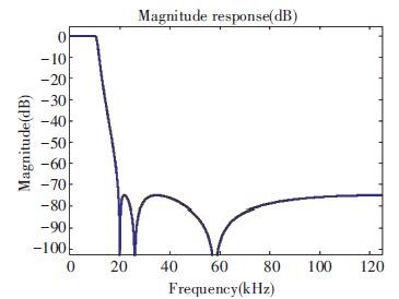
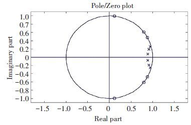
Traditionally there are four types of filter (Butterworth, ChebyshevⅠ, ChebyshevⅡ, and Elliptical) that can be selected in system-level design. Based on Simulink the four types are compared.The elliptic type has sharper rolloff in transition band than other types of the same order. In order to achieve the required rolloff speed the elliptic filter requires the least hardware consumption among the four types[12-13]. So, the elliptic filter is considered as the best choice. The SCF is designed by the filter design toolbox in Matlab in system level. Fig. 1 shows the frequency response of sixth-order elliptic filter. The stopband rejection is more than 70 dB. Poles and zeros of the sixth-order SCF system are also shown in Fig. 2. It is also obvious to view the stability of the system and the transfer function of the filter.
This transfer function of the filter is
|
$\begin{align}
& H\left( z \right)=[K\times ({{z}^{2}}-0.344\text{ }3z+1)\text{ }({{z}^{2}}-1.630\text{ }3z+1) \\
& \text{ }({{z}^{2}}-1.778\text{ }6z+1)\text{ }\left] / \right[({{z}^{2}}-1.804\text{ }1z+0.818\text{ }7) \\
& \text{ }({{z}^{2}}-1.839\text{ }4z+0.880\text{ }9)\text{ }({{z}^{2}}-1.894\text{ }7z+0.960\text{ }4)\text{ }] \\
\end{align}$
|
(1) |
Here, the parameter K is the gain of whole function and its value is 2.863×10⁻⁴. The sixth-order SCF can be realized by cascading three SC biquads which can realize complex combinations of zeros and poles facilely. According to the magnitude response of biquad filter, it can be divided into high quality factor (Q) and low quality factor structures. The high Q structure tends to lead to a more aggressing peaking in magnitude response than the low Q one. Since the high Q structure may cause oscillation and the low Q one may decrease stop-band rejection, it is necessary to arrange the combination of the sequence these different structures reasonably. By simulation, the order of the three biquads is low Q, high Q and low Q. Such order can provide insensitivity of element variations and small distribution of capacitors and avoid oscillation of the whole system[14]. The transfer functions of the three biquads are as follows:
|
${{H}_{1}}\left( z \right)={{K}_{1}}\frac{{{z}^{2}}-1.778\text{ }6z+1}{{{z}^{2}}-1.894\text{ }7z+0.960\text{ }4}$
|
(2) |
|
${{H}_{2}}\left( z \right)={{K}_{2}}\frac{{{z}^{2}}-1.630\text{ }3z+1}{{{z}^{2}}-1.839\text{ }4z+0.880\text{ }9}$
|
(3) |
|
${{H}_{3}}\left( z \right)={{K}_{3}}\frac{{{z}^{2}}+0.344\text{ }3z+1}{{{z}^{2}}-1.804\text{ }1z+0.818\text{ }7}$
|
(4) |
3 Transistor-level Design
Biquad is a common circuit structure in filter because it eases the difficulties of cascaded circuit. In this paper, the biquad circuit is used to realize the second-order filter. The common transfer function of a biquad circuit in Z-domain is
|
$H\left( z \right)=\frac{Vout\left( z \right)}{Vin\left( z \right)}=-\frac{{{a}_{2}}{{z}^{2}}+{{a}_{1}}z+{{a}_{0}}}{{{b}_{2}}{{z}^{2}}+{{b}_{1}}z+1}$
|
(5) |
where a0 , a1, a2, b1, b2 are the ratios of capacitors in the biquad structure. The sixth-order lowpass elliptic SCF realized by cascading three biquad structures is shown in Fig. 3. As is stated in system level design, the first and third levels are realized by biquad structure with high Q and the second level is realized by biquad structure with low Q. The values of the capacitors are calculated by three Eqs.(2) -(4) . The whole equation does not have only one solution, therefore it needs optimizing different combinations of capacitors many times, such as dynamic calibration in order to get high performance in terms of the output swing of each OTA.
3.1 The Design of OTA
The biquad is composed of two basic integrators as shown in Fig. 4. The switches are controlled by two non-overlapping clock φ1 and φ2. To analyze the effect of the finite gain and parasite capacitors in the real OTA, the expressions for Vout are shown in formulas (6) and (7) .
|
$\begin{align}
& Vouta\left( z \right)=\frac{{{C}_{s}}}{{{C}_{I}}}\left( 1/\left( 1+\left( 1+\frac{{{C}_{s}}}{{{C}_{I}}}+\frac{{{C}_{p}}}{{{C}_{I}}} \right)/{{A}_{dc}} \right) \right) \\
& \frac{{{z}^{-1}}\times Vin\left( z \right)}{1-\left( \left( {{A}_{dc}}+1+\frac{{{C}_{p}}}{{{C}_{I}}} \right)/\left( {{A}_{dc}}+1+\frac{{{C}_{s}}}{{{C}_{I}}}+\frac{{{C}_{p}}}{{{C}_{I}}} \right) \right){{z}^{-1}}} \\
\end{align}$
|
(6) |
|
$\begin{align}
& Voutb\left( z \right)=\frac{{{C}_{s}}}{{{C}_{I}}}\left( 1/\left( 1-\left( 1+\frac{{{C}_{p}}}{{{C}_{I}}} \right)/{{A}_{dc}} \right) \right) \\
& \frac{z\times Vin\left( z \right)}{1-\left( \left( {{A}_{dc}}-1-\frac{{{C}_{p}}}{{{C}_{I}}}-\frac{{{C}_{s}}}{{{C}_{I}}} \right)/\left( {{A}_{dc}}-1-\frac{{{C}_{p}}}{{{C}_{I}}} \right) \right)z}~ \\
\end{align}$
|
(7) |
where Cs is the sample capacitor; CI is the integrating capacitor; Cp is the parasite capacitor at the input of OTA and Adc represents the gain of OTA. It is obvious that as long as the gain is enough, the gain error and phase error introduced by the finite gain and parasite capacitor can be eliminated to great extent. Besides, the gain of OTA also affects the ripple of passband[12]:
|
$\Delta G=20lg(1+2Qmax/{{A}_{0}})$
|
(8) |
Here Qmax represents the quality factor of the filter.
When it comes to the setting error of the integrator, two performance indexes of OTA should be discussed: slew rate (SR) and gain band width (GBW). If the finite output current cannot drive the load capacitor during the integrating phase, it becomes the restraining factor in the integrator. So the SR should be[15]:
|
$SR>2\Delta {{V}_{out}}/{{T}_{S}}$
|
(9) |
where ΔVout means maximum output step of the integrator between two integrating phases. Otherwise, if the output current is large enough, the bandwidth becomes the main restraining factor. If the bandwidth is f0, the approximate setting error is:
|
$\varepsilon =\text{exp}(-T/(2{{f}_{0}}))$
|
(10) |
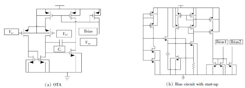
The minimum f0 should be seven times larger than Ts[16]. Aiming to achieve the relatively high gain, high slew rate and wide bandwidth, two-stage miller structure is selected. The biasing circuit with start-up-circuit for stable working at low power is also shown in Fig. 5. The performance of the OTA is listed in Table 1.
表 1

Table 1 Performance of OTA
| Gain | Bandwidth | Phase margin | Slew rate | Noise |
| 76.6 dB | 32.9 MHz( load capacitor 2pF) | 51° | 30 V/μs | 177 nv/Hz1/2(1 kHz) |
|
Table 1 Performance of OTA
|
3.2 Non-overlapping Clock and Analog Switch
Two pairs of non-overlapping clock are designed for the six-order SCF[17]. The structure of this non-overlapping clock is realized as shown in Fig. 6. The non-overlapping time should be as short as possible to avoid the charge leakage during the transition from one clock phase to the other clock phase.
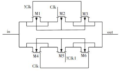
As shown in Fig. 7, a kind of switch made up of six MOS transistors is adopted in the filter. It can perform a lower on-resistance and have less to do with the input and output signal than PMOS or NMOS switches. Besides, the four dummy transistors can also reduce the influence caused by charge injection and clock feed-through[18].
3.3 Filter Simulation in Cadence and Layout
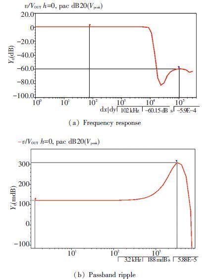
After all the statements above, the filter is realized in transistor level. It is simulated by Cadence with CSMC 0.5 μm CMOS technology[19]. For the clock frequency of 250 kHz, the simulation result is shown in Fig. 8. The corner frequency is 10 kHz, and the minimum stopband rejection is 60 dB and passband ripple is 0.19 dB.
After the design of circuit, the layout of the filter is finished. As the ratio of capacitors may affect the performance greatly, some special skills are adopted to lower the mismatch during fabrication. The taped out chip microphotograph in Fig. 9 shows the distributions of OTA, switches and capacitors. The effective area of the chip is 2.8 mm2.
4 Test Results
The filter is fabricated in CSMC 0.5 μm CMOS technology. Firstly, the CSMC technology corporation designs the masks based on the layout of the filter. Then each element of transistors and capacitors are etched on the basis of these masks. Finally, the whole circuit is fabricated on wafer. The test printed circuit board (PCB) is designed as shown in Fig. 10. It is powered by single 5 V supply and the clock for the filter is generated by function waveform generator. The filter is tested by Agilent 35670A. The frequency is swept from 1 Hz to 51 kHz and amplitude of the input signal is 1 V. The measured frequency response of the filter is shown in Fig. 11. The corner frequency is 10.6 kHz, and the minimum stopband rejection is 44 dB and passband ripple is 0.393 dB for the clock frequency of 250 kHz. There are deviations from the simulation results mainly because during the fabrication the ratio of capacitors cannot be controlled preciously although the layout tries to lower the mismatch. For example, during fabrication the masks can hardly reflect the layout without errors and the etching process may introduce random errors. Consequently there are some deviations from the ideal transfer function. The THD for a 1 kHz -8 dBV rms single ended input signal is about -64 dB. The measured in-band noise power is 4 μVrms/Hz1/2. The performance of the filter’s temperature drift is demonstrated in Fig. 12; the normalized corner frequency varies little, the maximum passband ripple is less than 0.49 dB and the minimum stopband rejection is over 40 dB for the temperature from -20 ℃ to 80 ℃. Meanwhile, the performance decreases with the increasing clock frequency and this is mainly because of the increasing setting error in the integrator during integrating phase.
The active area of the filter is 2.5 mm2 with 8 pads. It dissipates 10 mW from a 5 V supply voltage. The measurement results are shown in Table 2 to compare the performance with the previous reported test results. It is obvious that the filter gets a better performance than most of the reported filters in Table 2. It achieves lower THD than others.
5 Conclusions
In this paper, a 0.5 μm CMOS sixth-order low-pass elliptic switched-capacitor filter included in interface circuit of MEMS sensor is presented. The main design considerations have been discussed and applied to optimize the coefficients of the filter in terms of system stability, passband ripple and stopband rejection. The design combines simulation and statistical optimization at different levels of the filter. According to the experimental results this filter satisfies the implement in MEMS sensor. Compared with previous reports it achieves lower THD. Finally, it is also meaningful to lower its power consumption for low power application in MEMS sensors in the future.
表 2

Table 2 Performance summaries and comparisons
| Parameter | Ref.[1] | Ref. [9]* | Ref. [20] | Ref. [21]* | Ref. [22] | This work |
| Corner frequency (Hz) | 99.7 | 10 k | 3.4 M | 500 k | 2.4 | 10 k |
| Passband ripple (dB) | 0.14 | 0.5 | - | 1 | - | 0.49 |
| Stopband rejection (dB) | 78.6 | 40 | >30 | 60 | - | 40 |
| THD (dB) | - | - | -40 | - | <-50 | -64 |
| Output noise power | - | - | 0.97 μVrms/Hz1/2 | - | <50 μV(@ 0.1-2.4 Hz) | 4 μVrms/Hz1/2 |
| Voltage (V) | - | 1.8 | - | 1.8 | ±1.5 | 5 |
| Power dissipation (mW) | - | 0.374 4 | - | 0.85 | 0.01 | 10 |
| Process (μm) | 0.5 | 0.18 | 0.8 | 0.18 | 0.8 | 0.5 |
| Active area (mm2) | - | - | 1.44 | 1.175+ | 1 | 2 |
| * simulation data, + layout area. |
|
Table 2 Performance summaries and comparisons
|





 0)
0)
 0)
0)
 0)
0)
 0)
0)
 0)
0)
 0)
0)
 0)
0)
 0)
0)
 0)
0)
 0)
0)
 0)
0)
 0)
0)
 0)
0)
 0)
0)
 0)
0)
 0)
0)
 0)
0)
 0)
0)
 0)
0)
 0)
0)
 0)
0)
 0)
0)
 2016, Vol. 23


