In recent years, with the rapid development of power electronic converter technology, the demand for power electronic device of high voltage has become the research focus of converter technique. It is hoped that the device can withstand high voltage level and capacity level in converter technology, at the same time, can work under high switching frequency in order to reduce the harmonic content of output voltage[1-2]. With the advantages over two-level inverters of improved voltage waveform, smaller filter size and lower electromagnetic interference, three-level inverters are attracting a wide application.
Switching technique is an important factor for three-level inverters, so that the research of modulation scheme is prevailing at present. In Refs.[3-6], the carrier based PWM scheme is presented, but this scheme needs especially to generate carrier waves and use both EVs in DSP. Moreover, the switching frequency is relatively high and the utilization ratio of DC is low for this modulation technique. A space vector pulse width modulation (SVPWM) method is applied in Refs.[7-10]. This method can improve the utilization ratio of DC compared to PWM scheme, but it is a difficult task for DSP because of the complexity of the voltage vector space and region determination. In Refs.[11-13], a half cycle inversed based dual reference modulation three-level SPWM is proposed, which can be implemented by using only one EV in DSP and the attached logical circuit is no longer needed. However, the performance of output voltage is not improved. In order to further improve the output voltage waveform and reduce harmonic distortion, a novel wavelet modulation technique has been proposed. This new modulation technique is based on sampling sinusoidal reference modulating signals in a non-uniform recurrent process by using newly designed scaling function. This scaling function generates sets of wavelet basis functions which can construct nondyadic-type multi-resolution analysis. Furthermore, the continuous-time sinusoidal signals are reconstructed from their non-uniform recurrent samples by sets of synthesis scale-based linearly combined wavelet basis functions. Saleh[14-17] has introduced the development and implementation of WM technique for single-phase H-bridge inverters and three-phase VS six-pulse inverters. Simulation and experimental test results show that the proposed WM technique is able to switch two-level inverters to produce outputs with significantly improved fundamental components and low harmonic contents.
Based on the advantages of WM technique, the WM technique is extended from two-level inverters to three-level inverters in this paper. The developed three-level WM technique is also based on establishing a nondyadic MRA, which is capable of supporting the nonuniform recurrent sampling and reconstruction of CT sinusoidal signals[18-20]. Firstly, the paper briefly illustrates the principle of WM technique. Moreover, the developed WM technique for single-phase three-level voltage source inverter is proposed, and a step-by-step procedure for its implementation is detailed. In addition, the paper provides and discusses the simulated performance results of the WM technique in comparison with the PWM inverters for supplying the same load types. Then the output voltage of single-phase three-level voltage source inverter with WM is analyzed. By the theoretical analysis, the validity of the simulation results has been proved. At last, the experiment results of WM technique for single-level inverters prove its accuracy and feasibility.
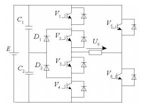
2 Wavelet Modulation TechniqueThe schematic diagram of the single-phase three-level inverter is shown in Fig. 1. Multi-level neutral-point-clamped voltage source inverter circuit has the characteristics of smaller control-tube withstand voltage. Based on the characteristic, the topology of single-phase three-level inverter circuit has been widely used in small or medium power applications.
|
Figure 1 Schematic diagram of six-switch three-level inverter |
The basis of the WM technique lies in the construction of a nondyadic multiresolution analysis (MRA) by using a new family of wavelet basis functions, which are called the scale-based linearly combined wavelet basis functions[10]. The wavelet basis functions {φ(2jt-k)} are generated by the scale-based linearly combined scaling function φ(t) at dilations j and translations k, and scaling function φ(t) can be defined at scale j as:
| $ {\varphi _j}\left( t \right) = {\phi _H}\left( {{2^{j + 1}}t} \right) + {\phi _H}\left( {{2^{j + 1}}\left( {t - 1 + {2^{ - \left( {j + 1} \right)}}} \right)} \right) $ | (1) |
where j=1, 2, 3, … and ϕH(t) is the Haar scaling function. The Haar scaling function is given by:
| $ {\phi _H}\left( t \right) = \left\{ \begin{array}{l} 1,t \in \left[ {0,1} \right)\\ 0,t \notin \left[ {0,1} \right] \end{array} \right. $ |
The wavelet basis functions create a group of two samples at each dilations j and translations k. For each cycle of the sinusoidal reference-modulating signal SM(t), a finite number of sample groups D are created. Sampling instants of each sample group are determined as follows:
| $ {t_{d1}} = T \cdot \left( {d + {2^{ - j - 1}}} \right)/D,{t_{d2}} = T \cdot \left( {d + 1 + {2^{ - j - 1}}} \right)/D $ | (2) |
where d=0, 1, 2, ..., D-1, T is the period of the reference-modulating signal SM(t).
The scale-based linearly combined synthesis scaling functions
| $ {{\tilde \varphi }_j}\left( t \right) = {\phi _H}\left( t \right) - {\varphi _j}\left( t \right) $ |
Defining S is the switching functions. When the switching is on, φj(t)=0 and S=1; when the switching is off, φj(t)=1 and S=0.
Fig. 2 shows that S varies with the change of the scale-based linearly combined scaling function φj(t).

|
Figure 2 Scaling functions and switching functions for WM |
The main idea of the WM technique is the construction of a nondyadic MRA process. The constructed nondyadic MRA which is the implementation of the wavelet modulation technique can be divided into two parts, which are as follows[6-10]:
(1) To sample the sinusoidal signal SM(t), which period is T, by nonuniform recurrent sampling. These nonuniform samples are created by the scaling functions φ(t) through specific dilation and translation. This part determines the position and width of the inverter switching pulse.
(2) Using the scale function to reconstruct the continuous recurrent signal in a series of nonuniform recurrent sampling from sinusoidal signal.This part produces the control signal of the inverter circuit switching devices.
3 Implementation of WM Technique for Operating Single-phase Three-level Voltage Source InverterThe wavelet modulation technique for operating a single-phase three-level voltage source inverter can be stated as a procedure with the following steps:
(1) Set the scale j to j0=1 and the index of sample groups d to d0=1.
(2) Create one group of two samples by using Eq.(2).
(3) Generate an ON switching pulse over the interval of the sample group d. In the positive half cycle, if t < T/8, ON switching pulse over the interval is as the control signal of V2, and this logical inversion is as the control signal of V4, while V1 is off and V3 is on; if T/8 < t < 3T/8, ON switching pulse over the interval is as the control signal of V1, and this logical inversion is as the control signal of V3, while V2 is on and V4 is off; if 3T/8 < t < T/2, the switching action is consistent with the former T/8. In the negative half cycle, if T/2 < t < 5T/8, ON switching pulse over the interval is as the control signal of V3, and this logical inversion is as the control signal of V1, while V2 is on and V4 is off; if 5T/8 < t < 7T/8, ON switching pulse over the interval is as the control signal of V4, and this logical inversion is as the control signal of V2, while V1 is off and V3 is on; if 7T/8 < t < T, the switching action is consistent with the former T/8 in the negative half cycle. Moreover, V5 is off and V6 is on in the positive half cycle, V5 is on and V6 is off in the negative half cycle.
(4) Evaluate S'M(t), if S'M(t)≥0, j=j+1; else j=j-1.
(5) If t≥T, then go to step (1); Otherwise d=d+1.
(6) Return to step (2) and calculate again. Among them, the sampling group d and scale parameter j satisfying relationship:
If 0 < t < T/4, d=j-1;
If T/4 < t < T/2, d=D/2-j;
If T/2 < t < 3T/4, d=D/2+j-1;
If 3T/4 < t < T, d=D-j.
4 Theoretical and Simulation Analysis 4.1 Theoretical Analysis of WM Output VoltageTo verify the correctness of a single-phase three-level inverter wavelet modulation strategy simulation, the theoretical analysis of the inverter output voltage is given. Usually the analysis is based on Fast Fourier Transformation to get the inverter output voltage amplitude and the harmonic frequency.
At the three-level bridge arm of compound single-phase three-level inverter, when the switch S1 and S2 both turned on, the output voltage of the bridge arm is E/2; when the switch S2 and S3 both turned on, the output voltage of the bridge arm is 0; when the switch S3 and S4 both turned on, the output voltage of the bridge arm is -E/2; Defining uAN as three-level bridge arm output voltage and N as the midpoint of two Capacitances Similarly, in the two-level bridge inverter circuit, when S5 turned on, the output voltage of the bridge arm is E/2; when S6 turned on, the output voltage of the bridge arm is -E/2; Defining uBN as two-level bridge arm output voltage. According to the wavelet modulation working principle of single-phase three-level inverter, in a sine wave modulation period, bridge arm output voltage uAN and uBN, can be expressed as follows:
| $ {u_{{\rm{AN}}}} = \left\{ \begin{array}{l} - \frac{E}{2},\frac{{dT}}{D} \le t \le {t_{d1}},{t_{d2}} \le t \le \frac{{\left( {d + 1} \right)T}}{D};t \in \left( {0,\frac{T}{8}} \right]{\rm{or}}\left( {\frac{{3T}}{8},\frac{T}{2}} \right]\\ \frac{E}{2},\;\;\;\;\;{t_{d1}} \le t \le {t_{d2}};t \in \left( {\frac{T}{8},\frac{{3T}}{8}} \right]\\ \frac{E}{2},\;\;\;\;\;\frac{{dT}}{D} \le t \le {t_{d1}},{t_{d2}} \le t \le \frac{{\left( {d + 1} \right)T}}{D};t \in \left( {\frac{T}{8},\frac{{5T}}{8}} \right]{\rm{or}}\left( {\frac{{7T}}{8},T} \right],\\ {u_{{\rm{BN}}}} = \left\{ \begin{array}{l} \frac{E}{2},\;\;\;\;t \in \left( {0,\frac{T}{2}} \right]\\ - \frac{E}{2},\;\;\;t \in \left( {\frac{T}{2},T} \right] \end{array} \right.\\ - \frac{E}{2},\;\;{t_{d1}} \le t \le {t_{d2}};t \in \left( {\frac{{5T}}{8},\frac{{7T}}{8}} \right]\\ 0,\;\;\;\;{\rm{others}};t \in \left( {0,T} \right] \end{array} \right. $ |
First of a single-phase three-level inverter three-level bridge arm output voltage Fourier decomposition, can be shown as follows:
| $ f\left( t \right) = {u_{{\rm{AN}}}} = {A_0} + \sum\limits_{k = 1}^\infty {\left[ {{a_k}\cos \left( {k\omega t} \right) + {b_k}\sin \left( {k\omega t} \right)} \right]} $ |
where ω=2π/T is angular frequency of the sinusoidal periodic function f(t); T is the period of f(t); A0 is the DC component. A0, ak, bk are Fourier coefficients, can be obtained by:
| $ \begin{array}{*{20}{c}} {{A_0} = \frac{1}{T}\int_0^{\rm{T}} {f\left( t \right){\rm{d}}t} }\\ {{a_k} = \frac{2}{T}\int_0^{\rm{T}} {f\left( t \right)\cos \left( {k\omega t} \right){\rm{d}}t} }\\ {{b_k} = \frac{2}{T}\int_0^{\rm{T}} {f\left( t \right)\sin \left( {k\omega t} \right){\rm{d}}t} } \end{array} $ |
UAN is the effective value of three-level bridge arm output voltage; UA1 is the Fundamental wave effective value of the bridge arm output voltage; UAk is the effective value of harmonic component, where k is the harmonic frequency; UAH is effective value of total harmonic. UAN and UAH can be expressed as:
| $ \begin{array}{l} {U_{{\rm{AN}}}} = \sqrt {\frac{1}{T}\int_0^{\rm{T}} {{{\left[ {f\left( t \right)} \right]}^2}{\rm{d}}t} } = \sqrt {\frac{1}{T}\int_0^{\rm{T}} {{{\left[ {{u_{{\rm{AN}}}}} \right]}^2}{\rm{d}}t} } \\ \;\;\;\;\;\;\; = \sqrt {A_0^2 + \sum\limits_{k = 1}^\infty {U_{{\rm{A}}\mathit{k}}^2} } \\ {U_{{\rm{AH}}}} = \sqrt {\sum\limits_{k = 2}^\infty {U_{{\rm{A}}\mathit{k}}^2} } \end{array} $ |
Output voltage of inverter three-level bridge arm, fundamental component is the desired output sine wave, the rest of the component of the expression can be regarded as output voltage harmonic distortion, so the represents of quality of the inverter circuit output voltage rate of total harmonic distortion (THD) can be shown by the following type:
| $ \begin{array}{l} THD = \sqrt {{{\left( {\frac{{{A_0}}}{{{U_{A1}}}}} \right)}^2} + \sum\limits_{k = 1}^\infty {{{\left( {\frac{{{U_{{\rm{A}}\mathit{k}}}}}{{{U_{{\rm{A1}}}}}}} \right)}^2}} } = \sqrt {{{\left( {\frac{{{U_{{\rm{A}}\mathit{k}}}}}{{{U_{{\rm{A1}}}}}}} \right)}^2} - 1} ,\\ \;\;\;\;{a_k} = 0\\ {b_k} = \frac{2}{T}\int_0^T {f\left( t \right)\sin \left( {k\omega t} \right){\rm{d}}t} = - \frac{1}{{k{\rm{ \mathsf{ π} }}}}\left[ {f\left( t \right)\cos \left( {k\omega t} \right)} \right]_0^T = \\ - \frac{1}{{k{\rm{ \mathsf{ π} }}}}\left\{ { - \frac{E}{2}\sum\limits_{d = 0}^{{D_1}} {\left( {\cos \left( {k\omega \frac{{\left( {d + 1} \right)T}}{D}} \right) - \cos \left( {k\omega {t_{d2}}} \right)} \right.} } \right. + \\ \left. {\cos \left( {k\omega {t_{d1}}} \right) - \cos \left( {k\omega \frac{{dT}}{D}} \right)} \right) + \frac{E}{2}\sum\limits_{d = {D_1}}^{{D_2}} {\left( {\cos \left( {k\omega {t_{d2}}} \right)} \right.} - \\ \left. {\cos \left( {k\omega {t_{d1}}} \right)} \right) - \frac{E}{2}\sum\limits_{d = {D_2}}^{{D_3}} {\left( {\cos \left( {k\omega \frac{{\left( {d + 1} \right)T}}{D}} \right) - } \right.} \\ \left. {\cos \left( {k\omega {t_{d2}}} \right) + \cos \left( {k\omega {t_{d1}}} \right) - \cos \left( {k\omega \frac{{dT}}{D}} \right)} \right) + \\ \frac{E}{2}\sum\limits_{d = {D_3}}^{{D_4}} {\left( {\cos \left( {k\omega \frac{{\left( {d + 1} \right)T}}{D}} \right) - \cos \left( {k\omega {t_{d2}}} \right) + } \right.} \\ \left. {\cos \left( {k\omega {t_{d1}}} \right) - \cos \left( {k\omega \frac{{dT}}{D}} \right)} \right) - \frac{E}{2}\sum\limits_{d = {D_3}}^{{D_4}} {\left( {\cos \left( {k\omega {t_{d2}}} \right) - } \right.} \\ \left. {\cos \left( {k\omega {t_{d1}}} \right)} \right) + \frac{E}{2}\sum\limits_{d = {D_5}}^D {\left( {\cos \left( {k\omega \frac{{\left( {d + 1} \right)T}}{D}} \right) - } \right.} \\ \left. {\cos \left( {k\omega {t_{d2}}} \right) + \left. {\cos \left( {k\omega {t_{d1}}} \right) - \cos \left( {k\omega \frac{{dT}}{D}} \right)} \right)} \right\} \end{array} $ |
where D1 is the biggest sampling group when t∈(0, T/8]; D2 is the biggest sampling group when t∈(T/8, 3T/8]; D3 is the biggest sampling group when t∈(3T/8, T/2]; D4 is the biggest sampling group when t∈ T/2, 5T/8; D5 is the biggest sampling group when t∈ 5T/8, 7T/8.
Using the above calculation of bk, we can get the Fourier series expansion of uAN:
| $ f\left( t \right) = {u_{{\rm{AN}}}} = \sum\limits_{k = 1}^\infty {{b_k}\sin \left( {k\omega t} \right)} $ |
In the same way, the two-level bridge arm Fourier decomposition expression of the output voltage uBN is shown as follows:
| $ g\left( t \right) = {u_{{\rm{AN}}}} = {B_0} + \sum\limits_{k = 1}^\infty {\left[ {{c_k}\cos \left( {k\omega t} \right) + {d_k}\sin \left( {k\omega t} \right)} \right]} $ | (3) |
| $ \begin{array}{l} {c_k} = 0\\ {d_k} = \frac{2}{T}\int_0^T {g\left( t \right)\sin \left( {k\omega t} \right){\rm{d}}t} = - \frac{1}{{k{\rm{ \mathsf{ π} }}}}\left[ {g\left( t \right)\cos \left( {k\omega t} \right)} \right]_0^T = \\ \;\;\;\;\;\; - \frac{1}{{k{\rm{ \mathsf{ π} }}}}\left[ { - \frac{E}{2}\left( {\cos \left( {k\omega \frac{T}{2}} \right) - \cos \left( {k\omega \cdot 0} \right)} \right)} \right. + \\ \;\;\;\;\;\;\left. {\frac{E}{2}\left( {\cos \left( {k\omega t} \right) - \cos \left( {k\omega \frac{T}{2}} \right)} \right)} \right] = \frac{E}{{k{\rm{ \mathsf{ π} }}}}\left[ {\cos \left( {k{\rm{ \mathsf{ π} }}} \right)} \right. - \\ \;\;\;\;\;\;\left. 1 \right] = \frac{E}{{k\omega }}\left[ {{{\left( { - 1} \right)}^k} - 1} \right] = \left\{ \begin{array}{l} - \frac{{2E}}{{k{\rm{ \mathsf{ π} }}}},\;\;\;\;k = 1,3,5 \cdots \\ 0,\;\;\;\;\;\;\;\;\;k = 2,4,6 \cdots \end{array} \right. \end{array} $ |
Using the above calculation of bk, we can get the Fourier series expansion of uBN:
| $ \begin{array}{l} g\left( t \right) = {u_{{\rm{BN}}}} = \sum\limits_{k = 1}^\infty {{d_k}\sin \left( {k\omega t} \right)} = - \frac{{2E}}{{\rm{ \mathsf{ π} }}}\left[ {\sin \left( {\omega t} \right) + } \right.\\ \;\;\;\;\;\;\;\;\;\;\frac{1}{3}\sin \left( {3\omega t} \right) + \frac{1}{5}\sin \left( {5\omega t} \right) + \cdots + \\ \;\;\;\;\;\;\;\;\;\;\left. {\frac{1}{k}\sin \left( {k\omega t} \right) + \cdots } \right] \end{array} $ | (4) |
From Eqs.(3) and (4), we can get output voltage Fourier decomposition expression of a single-phase three-level inverter:
| $ \begin{array}{l} {u_0} = {u_{{\rm{AN}}}} - {u_{{\rm{BN}}}} = \sum\limits_{k = 1}^\infty {{b_k}\sin \left( {k\omega t} \right)} - \sum\limits_{k = 1}^\infty {{d_k}\sin \left( {k\omega t} \right)} = \\ \;\;\;\;\;\;\;\sum\limits_{k = 1}^\infty {\left[ {\left( {{b_k} - {d_k}} \right)\sin \left( {k\omega t} \right)} \right]} \end{array} $ | (5) |
By the Fourier decomposition expression of a single-phase three-level inverter output voltage u0, the fundamental voltage component of u0 and voltage total harmonic distortion rate can be obtained. The total harmonic distortion rate expression is shown as follows:
| $ THD = \sqrt {\sum\limits_{k = 2}^\infty {{{\left( {\frac{{{U_{0k}}}}{{{\mathit{U}_{01}}}}} \right)}^2}} } = \sqrt {{{\left( {\frac{{{U_0}}}{{{\mathit{U}_{01}}}}} \right)}^2} - 1} $ | (6) |
By Eqs.(5) and (6), the theoretical value of the output voltage amplitude value and the total harmonic distortion (THD) of a single-phase three-level inverter under wavelet modulation strategy can be calculated.
4.2 Simulation Analysis of WM Output VoltageThe simulation circuit model of a single-phase three-level voltage source inverter is constructed based on Matlab/Simulink and the experiment is performed on the DSP hardware platform. To generate high quality control signals, the WM algorithm is implemented by DSP TMS320F2812. Furthermore, the dead time should be set between two complementary switches, V1 and V3, V2 and V4, V5 and V6, respectively. The DC input is supplied by a 40 V voltage source and the load is 10 Ω resistance.
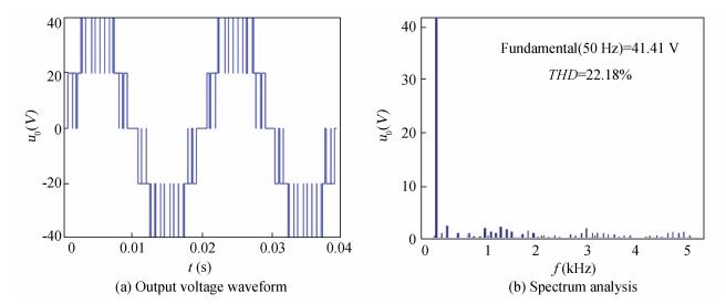
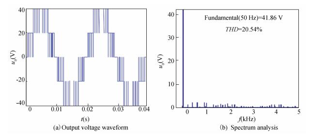
Based on the wavelet modulation, the MATLAB simulation analysis of a single-phase three-level inverter is given below; the simulation parameters are the same as SPWM. When sample groups D take different values, modulation frequency f=50 Hz, the simulation of the output voltage waveform and spectrum analysis are given below. When sampling groups D=30 and 40, the simulation waveforms are shown in Fig. 3 and Fig. 4.
|
Figure 3 Single-phase three-level inverter WM output voltage and frequency spectrum (D=30) |
|
Figure 4 Single-phase three-level inverter WM output voltage and frequency spectrum (D=40) |
Then to compare the theoretical value with the simulation results, the analysis results are shown in Table 1.
| Table 1 Wavelet modulation theoretical value compared with the simulation values |
From Table 1, the simulation results of the fundamental voltage component of u0 and the total harmonic distortion THD are similar to the theoretical value. Proved the simulation results of a single-phase three-level inverter wavelet modulation strategy are correct.
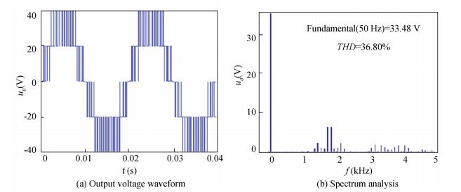
For the purpose of performance comparisons, the PWM technique is simulated for supplying the same load. The PWM technique is implemented with a carrier frequency of fc=1.8 kHz and a modulation index of ma=0.85. The simulation waveform is shown in Fig. 5.
|
Figure 5 Single-phase three-level inverter SPWM output voltage and frequency spectrum |
Table 2 summarizes the magnitudes of output voltage fundamental components (|U0|) and voltage total harmonic distortion (THD) for the SPWM and WM with different sample groups D.
| Table 2 Simulated performance comparisons between the WM and SPWM |
It is easy to find out that the amplitude of WM output fundamental voltage with D=36 is 41.41 V, while the amplitude of SPWM output fundamental voltage with a carrier frequency of fc=1.8 kHz and a modulation index of ma=0.85 is 33.48 V. So, with the input voltage DC=40 V, the DC voltage utilization of WM is 1.035, and that of SPWM is 0.837. Then, the DC voltage utilization of WM is higher and better than SPWM.
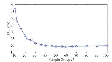
The simulated performances show that a single-phase three-level voltage source inverter with wavelet modulation strategy has smaller output voltage harmonic contents, larger amplitude, and lower switching frequency than SPWM. At the same time, the WM is simple and easy to implement. Further, it can be seen from Table 2 that there is a certain relationship between output voltage total harmonic distortion and sampling group D. The simulation analysis was made on different number of sample group D. Fig. 6 shows the relationship between D and total harmonic distortion.
From Fig. 6, it can be concluded that the sample group D in wavelet modulation and voltage total harmonic distortion is nonlinear relationship. When the number of sample group D has increased from 10 to 60, the output voltage total harmonic distortion gradually decreases; when the number of sampling group D has increased from 60 to 100, the output voltage total harmonic distortion gradually increases. So, the appropriate number of sample group D should not be larger than 60. In practice, it is necessary to take into account to the operating frequency of switching devices, switch loss, and output total voltage harmonic distortion. Therefore, the number of sample group D usually ranges between 30 to 50. In conclusion, in wavelet modulation strategy, to select the appropriate number of sample group D, so the switch frequency of inverter, switching losses and total harmonic distortion will be very small, and can effectively improve the wavelet modulation inverter output characteristics.
|
Figure 6 The relationship between sample group D and total harmonic distortion |
5 Wavelet Modulation Experimental Results
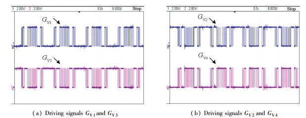
For the reason of a complete performance demonstration, the step-by-step procedure of implementation the single-phase three-level WM technique is performed on the DSP hardware platform. To generate high quality control signals, the WM algorithm is implemented by DSP TMS320F2812. Furthermore, the dead time should be set between two complementary switches. Then the driving signals are shown in Fig. 7. The DC input is supplied by a 40 V voltage source and the load is 10 Ω resistances.
|
Figure 7 Driving signals with the dead time |
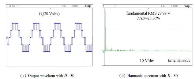
The experimental results are shown in Fig. 8. It can be seen that the frequency of the output voltage is 50 Hz. Fig. 8(a) shows the single-phase three-level output voltage waveform with sample group D=30, Fig. 8(b) shows the harmonic spectrum of the output voltage with sample group D=30.
|
Figure 8 Experiment waveforms of WM scheme D=30 |
The experimental results are shown in Fig. 9. It can be seen that the frequency of the output voltage is 50 Hz. Fig. 9(a) shows the single-phase three-level output voltage waveform with sample group D=40, and Fig. 9(b) shows the harmonic spectrum of the output voltage with sample group D=40.

|
Figure 9 Experiment waveforms of WM scheme D=40 |
To compare the simulation value with the experimental value, the results of fundamental voltage component and the THD of output voltage have been shown in Table 3.
| Table 3 Comparisons between simulation results and experimental results |
From Table 3, the experimental results of the fundamental voltage component of u0 and the total harmonic distortion THD are similar to the simulation value. Proved the experimental results of a single-phase three-level inverter wavelet modulation strategy are correct.
6 ConclusionsAs the analysis of the wavelet modulation strategy applying on the single-phase three-level voltage source inverter, the theoretical analysis is proved correctly by the simulation value. And the experimental results show that the wavelet modulation strategy can be achieved and be also similar to the theoretical and simulation value. Compared with the SPWM, the single-phase three-level voltage source inverter shows that high magnitude of fundamental components and significantly reduced harmonic contents of the inverter outputs can be achieved by using WM. Furthermore, the hardware implementation of the WM scheme can be easily realized with only one EV in DSP. The simulated and experimental results prove its accuracy and feasibility.
| [1] |
Kouro S, Rodrigucz J, Rebolledo J. Reduced switching frequency modulation algorithm for high-power multilevel inverters.
IEEE Transaction on Industrial Electronics, 2007, 54(5): 2894-2901.
DOI:10.1109/TIE.2007.905968 ( 0) 0)
|
| [2] |
Lee Seung-Joo, Lee June-Seok, Lee Kyo-Beum. Novel switching strategy for high-efficiency of single-phase three-level inverters. IEEE Conference on Energy Conversion, 2014. 342-347.
( 0) 0)
|
| [3] |
Zhu W J, Zhou K L, Cheng M, et al. PWM modulated three-level single-phase grid-connected PV inverter. IEEE Int. Electrical Machines and Systems Conf., Beijing, 2011. 1-3.
( 0) 0)
|
| [4] |
Xiao Huafeng, Xie Shaojun. Transformerless split-inductor neutral point clamped three-level PV grid-connected inverter.
IEEE Transactions on Power Electronics, 2012, 27(4): 1799-1808.
DOI:10.1109/TPEL.2011.216490 ( 0) 0)
|
| [5] |
Liu Z C, Kong P J, Wu X Z, et al. Implementation of DSP based three-level inverter with dead time compensation. IEEE Int. Power Electronics and Motion Control Conf., Xi'an, 2004. 782-787.
( 0) 0)
|
| [6] |
Ben Bing, Zhang Xiubei, Kan Zhizhong, et al. Improved repetitive control of single-phase three-level inverter based on PWM voltage feedback. Electronics and Application Conference and Exposition (PEAC), 2014. 1328-1332.
( 0) 0)
|
| [7] |
Zhang Z, Xie Y X, Huang W P, et al. A new SVPWM method for single-phase three-level NPC inverter and the control method of neutral point voltage balance. IEEE Int. Electrical Machines and Systems Conf., Tokyo, 2009. 1-4.
( 0) 0)
|
| [8] |
Wu F J, Sun B, Peng H R. Single-phase three-level SPWM scheme suitable for implementation with DSP.
Electronics Letters, 2011, 47(17): 994-996.
DOI:10.1049/el.2011.1969 ( 0) 0)
|
| [9] |
Lin Lei, Zou Yunping, Zou Xudong. Digital implementation of diode-clamped three-phase three-level SVPWM inverter. The Fifth International on Power Electronics and Drive Systems. Piscataway:IEEE, 2003. 1413-1417.
( 0) 0)
|
| [10] |
Han Yaofei, Fan Xiaohong, Zhao Zhangfei. The study and realization of three-level SVPWM algorithm for high power inverter. IEEE International Conference on Electrical and Control Engineering. Piscataway:IEEE, 2011. 6177-6180.
( 0) 0)
|
| [11] |
Srirattanawichaikul W, Kumsuwan Y, Premrudeepreechacharn S, et al. A carrier based PWM strategy for three-level neutral-point-clamped voltage source inverters. IEEE Ninth International Conference on Power Electronics and Drive Systems. Piscataway:IEEE, 2011. 948-951.
( 0) 0)
|
| [12] |
Dordevic O, Jones M, Levi E. A comparison of carrier-based and space vector PWM techniques for three-level five-phase voltage source inverters.
IEEE Transactions on Industrial Informatics, 2012, 9(2): 609-619.
DOI:10.1109/TII.2012.2220553 ( 0) 0)
|
| [13] |
Das S, Narayanan G. Novel switching sequences for a space-vector-modulated three-level inverter.
IEEE Transactions on Industrial Electronics, 2012, 59(3): 1477-1487.
DOI:10.1109/TIE.2011.2163373 ( 0) 0)
|
| [14] |
Saleh S A, Rahman M A. Experimental performances of the single-phase wavelet-modulated inverter.
IEEE Transactions on Power Electronics, 2011, 26(9): 2650-2661.
DOI:10.1109/TPEL.2011.2122344 ( 0) 0)
|
| [15] |
Saleh S A, Rahman M A. Development and testing of a new controlled wavelet-modulated inverter for IPM motor drives.
IEEE Transactions on Industry Applications, 2010, 46(4): 1630-1643.
DOI:10.1109/TIA.2010.2049814 ( 0) 0)
|
| [16] |
Saleh S A, Moloney C R, Rahman M A. Analysis and development of wavelet modulation for three phase voltage source inverters.
IEEE Transactions on Industrial Electronics, 2011, 58(8): 3330-3348.
DOI:10.1109/TIE.2010.2081957 ( 0) 0)
|
| [17] |
Saleh S A, Rahman M A. Development and experimental validation of resolution-level controlled wavelet modulated inverters for three-phase induction motor drives.
IEEE Transactions on Industry Applications, 2011, 47(4): 1958-1970.
DOI:10.1109/TIA.2011.2156375 ( 0) 0)
|
| [18] |
Saleh S A, Cecilia R M. Development and testing of wavelet modulation for single-phase inverters.
IEEE Trans. Ind. Electron., 2009, 56(7): 2588-2599.
DOI:10.1109/TIE.2009.2019776 ( 0) 0)
|
| [19] |
Saleh S A, Scaplen B, Rahman M A. A new implementation method of wavelet-packet-transform differential protection for power transformers.
IEEE Transaction on Industry Application, 2011, 47(2): 1003-1012.
DOI:10.1109/TIA.2010.2103545 ( 0) 0)
|
| [20] |
Saleh S A. The implementation and performance evaluation of 3φ VS wavelet modulated AC-DC converters.
IEEE Transactions on Power Delivery, 2012, 28(3): 1096-1106.
DOI:10.1109/TPEL.2012.2205945 ( 0) 0)
|
 2017, Vol. 24


