1 Introduction As a hot spot and a new growth point of the global information technology industry development, mobile intelligent terminal is still at the early stages of development. After years of development, the domestic mobile intelligent terminal industry chain gradually trends perfect. Meanwhile, more and more continuous innovation has propelled the domestic market improvement with the international market. With the local 4G LTE licenses issued, more opportunities and challenges are instilling a new energy into the market. As for verifying intelligent terminal integrated circuit (IC)'s quality, S parameter is introduced as one of the crucial parameters. Therefore, the S parameter calibration method becomes important to RF IC and system testing on mobile intelligent terminal. Though S parameter can be accurately tested on wafer level through the precise vector net analyzer (VNA), S parameter measurement on COB level is necessary to be applied due to the terminal application and high power non-linear distortion verification. Therefore, the parasitic effects on the COB will confuse the results[1-2]. Based on different requirements, some calibration methods have been proposed on different error model nets analysis, such as Short-Open-Load-Thru (SOLT)[3], Thru-Reflect-Line (TRL), Line-Reflect-Reflect-Match (LRRM)[4], and etc[5-9]. At present, the popular de-embedding method is applied in wafer level test using Cascade probes and impedance standard substrate (ISS)[10].
However, COB level calibration method is not well resolved because it is difficult to change the calibration plane to the actual device without SMA connectors. Mubarak et al.[1] solved the inevitable cable flexure issue with the electronic calibration units (ECU) calibration method. But it is difficult to extend to the reference plan on chip. He and Jiang[11] had raised the research on S parameter measurement of surface mounting device (SMD). But it has many limitations, for instance, only TRL with thru structure could be utilized. It could not cover distinct ports issue. Therefore, this paper focuses on one-port calibration method which is extended OSL[12] to verify the best way to do COB de-embedding. Three-level cascade structure on COB's system error model is proposed and analyzed. Four kinds of calibration solutions are verified. They are named as on-board CAL kits, thru trace with standard CAL kits, trace with bonding wire and standard CAL kits and CAL kits only. All experiments are set up on Advantest 93 K tester with Agilent standard CAL kits. As a result, on-board CAL kits solution is established for application and for decreasing the system error to the least value that the max error shift could be controlled less than 0.1 dB.
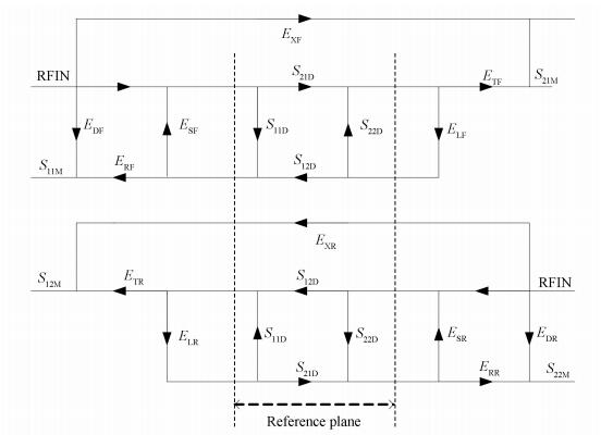
2 S parameter Calibration Theory Before an accuracy measurement, the test system is necessary to be calibrated. An RF testing system concludes two types of errors that are called random and systematic errors. Usually, error calibration includes response calibration and vector calibration. Vector calibration method which has one-port and two-port calibrations is the most popular in S parameter calibration method. In order to explain and analyze the error model, Fig. 1 lists the common error model and Table 1 shows the detailed meaning on the error model[13-14].
表 1

Table 1 Significance on error model
| Error coefficient |
Physical significance |
| Forward |
Reverse |
| EDF |
EDR |
Directivity |
| ESF |
ESR |
Source match |
| EXF |
EXR |
Isolation |
| ETF |
ETR |
Transmission tracking |
| ERF |
ERR |
Reflection tracking |
| ELF |
ELR |
Load match |
|
Table 1 Significance on error model
|
The completed error model is defined as directivity error, source match error, isolation error, transmission tracking error, reflection tracking error and load match error. The first subscript stands for character of error term and the second subscript stands for stimulus direction. For example, the “X” in “EXF” means isolation error and “F” in “EXF” means forward stimulus. Based on the Mason rule and S parameter measured (S11M, S12M, S21M, S22M), the exact S parameter (S11D, S12D, S21D, S22D) of device under test (DUT) can be modified and calculated. For reference, the calibration Eqs.(1)-(4) are listed as follows[15]:
|
$
{S_{11{\rm{D}}}} = \\\frac{{\left\{ {\left( {\frac{{{S_{11{\rm{M}}}} - {E_{{\rm{DF}}}}}}{{{E_{{\rm{RF}}}}}}} \right)\left[ {1 + \left( {\frac{{{S_{22{\rm{M}}}} - {E_{{\rm{DR}}}}}}{{{E_{{\rm{RR}}}}}}} \right){E_{{\rm{SR}}}}} \right]} \right\} - \left[ {\left( {\frac{{{S_{21{\rm{M}}}} - {E_{{\rm{XF}}}}}}{{{E_{{\rm{TF}}}}}}} \right)\left( {\frac{{{S_{12{\rm{M}}}} - {E_{{\rm{XR}}}}}}{{{E_{{\rm{TR}}}}}}} \right){E_{{\rm{LF}}}}} \right]}}{{\left[ {1 + \left( {\frac{{{S_{11{\rm{M}}}} - {E_{{\rm{DF}}}}}}{{{E_{{\rm{RF}}}}}}} \right){E_{{\rm{SF}}}}} \right]\left[ {1 + \left( {\frac{{{S_{22{\rm{M}}}} - {E_{{\rm{DR}}}}}}{{{E_{{\rm{RR}}}}}}} \right){E_{{\rm{SR}}}}} \right] - \left[ {\left( {\frac{{{S_{21{\rm{M}}}} - {E_{{\rm{XF}}}}}}{{{E_{{\rm{TF}}}}}}} \right)\left( {\frac{{{S_{12{\rm{M}}}} - {E_{{\rm{XR}}}}}}{{{E_{{\rm{TR}}}}}}} \right){E_{{\rm{LF}}}}{E_{{\rm{LR}}}}} \right]}}
$
|
(1) |
|
$
{S_{21{\rm{D}}}} = \\\frac{{\left[ {1 + \left( {\frac{{{S_{22{\rm{M}}}} - {E_{{\rm{DR}}}}}}{{{E_{{\rm{RR}}}}}}} \right)\left( {{E_{{\rm{SR}}}} - {E_{{\rm{LR}}}}} \right)} \right]\left( {\frac{{{S_{21{\rm{M}}}} - {E_{{\rm{XF}}}}}}{{{E_{{\rm{TF}}}}}}} \right)}}{{\left[ {1 + \left( {\frac{{{S_{11{\rm{M}}}} - {E_{{\rm{DF}}}}}}{{{E_{{\rm{RF}}}}}}} \right){E_{{\rm{SF}}}}} \right]\left[ {1 + \left( {\frac{{{S_{22{\rm{M}}}} - {E_{{\rm{DR}}}}}}{{{E_{{\rm{RR}}}}}}} \right){E_{{\rm{SR}}}}} \right] - \left[ {\left( {\frac{{{S_{21{\rm{M}}}} - {E_{{\rm{XF}}}}}}{{{E_{{\rm{TF}}}}}}} \right)\left( {\frac{{{S_{12{\rm{M}}}} - {E_{{\rm{XR}}}}}}{{{E_{{\rm{TR}}}}}}} \right){E_{{\rm{LF}}}}{E_{{\rm{LR}}}}} \right]}}
$
|
(2) |
|
$
{S_{12{\rm{D}}}} = \\\frac{{\left[ {1 + \left( {\frac{{{S_{11{\rm{M}}}} - {E_{{\rm{DR}}}}}}{{{E_{{\rm{RR}}}}}}} \right)\left( {{E_{{\rm{SR}}}} - {E_{{\rm{LR}}}}} \right)} \right]\left( {\frac{{{S_{21{\rm{M}}}} - {E_{{\rm{XR}}}}}}{{{E_{{\rm{TR}}}}}}} \right)}}{{\left[ {1 + \left( {\frac{{{S_{11{\rm{M}}}} - {E_{{\rm{DF}}}}}}{{{E_{{\rm{RF}}}}}}} \right){E_{{\rm{SF}}}}} \right]\left[ {1 + \left( {\frac{{{S_{22{\rm{M}}}} - {E_{{\rm{DR}}}}}}{{{E_{{\rm{RR}}}}}}} \right){E_{{\rm{SR}}}}} \right] - \left[ {\left( {\frac{{{S_{21{\rm{M}}}} - {E_{{\rm{XF}}}}}}{{{E_{{\rm{TF}}}}}}} \right)\left( {\frac{{{S_{12{\rm{M}}}} - {E_{{\rm{XR}}}}}}{{{E_{{\rm{TR}}}}}}} \right){E_{{\rm{LF}}}}{E_{{\rm{LR}}}}} \right]}}
$
|
(3) |
|
$
{S_{22{\rm{D}}}} = \\\frac{{\left\{ {\left( {\frac{{{S_{22{\rm{M}}}} - {E_{{\rm{DR}}}}}}{{{E_{{\rm{RR}}}}}}} \right)\left[ {1 + \left( {\frac{{{S_{11{\rm{M}}}} - {E_{{\rm{DR}}}}}}{{{E_{{\rm{RR}}}}}}} \right){E_{{\rm{SF}}}}} \right]} \right\} - \left[ {\left( {\frac{{{S_{21{\rm{M}}}} - {E_{{\rm{XF}}}}}}{{{E_{{\rm{TF}}}}}}} \right)\left( {\frac{{{S_{12{\rm{M}}}} - {E_{{\rm{XR}}}}}}{{{E_{{\rm{TR}}}}}}} \right){E_{{\rm{LR}}}}} \right]}}{{\left[ {1 + \left( {\frac{{{S_{11{\rm{M}}}} - {E_{{\rm{DF}}}}}}{{{E_{{\rm{RF}}}}}}} \right){E_{{\rm{SF}}}}} \right]\left[ {1 + \left( {\frac{{{S_{22{\rm{M}}}} - {E_{{\rm{DR}}}}}}{{{E_{{\rm{RR}}}}}}} \right){E_{{\rm{SR}}}}} \right] - \left[ {\left( {\frac{{{S_{21{\rm{M}}}} - {E_{{\rm{XF}}}}}}{{{E_{{\rm{TF}}}}}}} \right)\left( {\frac{{{S_{12{\rm{M}}}} - {E_{{\rm{XR}}}}}}{{{E_{{\rm{TR}}}}}}} \right){E_{{\rm{LF}}}}{E_{{\rm{LR}}}}} \right]}}
$
|
(4) |
Isolation term measurement will reveal the crosstalk error term. Sometimes, we also ignore the isolation term because its result is much smaller than connector repeatability error. Therefore, we can transfer the 12 error model to 10 error model. Thereby, the complex calculation can be decreased as well. Based on the study in Ref.[12], it shows that extended OSL can reach the same accuracy as the SOLT calibration method for practical application[12]. Meanwhile, it also solves the distinct ports issue. Therefore, the following paper conducts the experiments based on extended OSL method. The purpose is to do the COB three-level cascade structure model[16] de-embedding research.
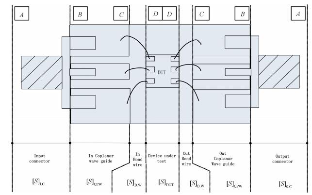
3 Model on COB Package Among a number of cascade de-embedding approaches, thru-only method[17-18] and their variants[19-21] seem to be gaining popularity. In this case, each COB section of the COB test fixture can be individually characterized by its S parameter and then cascaded for the complete in-fixture response. Hence, every COB section is defined as several sub-nets. For this purpose, we convert the [S] matrices to [T] matrices and multiply them together in a chain fashion. Discontinuities at the interfaces are sure to be considered, since they generate reflections. Fig. 2 shows the basic COB package model. Different [S] matrices can be also equivalent to signal flow graph which is convenient to be analyzed.
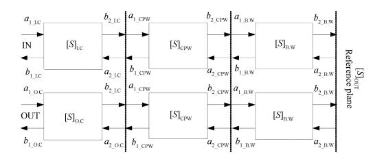
During the test, the COB which includes die, bond wire and fixture carrier all acts as a single RF assembly. Four reference planes can be defined as connector reference plane AB, carrier reference plane BC, bonding/cavity reference plane CD and die reference plane DD. Therefore, the de-embedding solution is set up based on the COB model. In the above model, wave continuity should be paid attention to or the reflection influence will be brought from connector reference plane, carrier reference and bonding/cavity reference plane. Fig. 3 shows the S parameter model on COB which is three-level cascade structure. Because the cascade two-port network is difficult to use S parameter, we adopt the T parameter model for detail analysis.
According to the sub-net, input connector model Eq.(5) is listed as follows:
|
$
\left[ {\begin{array}{*{20}{c}}
{{b_{1\_{\rm{I}}{\rm{.C}}}}}\\
{{a_{1\_{\rm{I}}{\rm{.C}}}}}
\end{array}} \right] = \left[ {\begin{array}{*{20}{c}}
{{{T'}_{11}}}&{{{T'}_{12}}}\\
{{{T'}_{21}}}&{{{T'}_{22}}}
\end{array}} \right] \cdot \left[ {\begin{array}{*{20}{c}}
{{a_{2\_{\rm{I}}{\rm{.C}}}}}\\
{{b_{2\_{\rm{I}}{\rm{.C}}}}}
\end{array}} \right] = \left[ {{T_{{\rm{I}}{\rm{.C}}}}} \right] \cdot \left[ {\begin{array}{*{20}{c}}
{{a_{2\_{\rm{I}}{\rm{.C}}}}}\\
{{b_{2\_{\rm{I}}{\rm{.C}}}}}
\end{array}} \right]
$
|
(5) |
By the same token, input coplanar wave guide (CPW) and input bonding wire (B.W) model Eqs.(6) and (7) are listed:
|
$
\left[ {\begin{array}{*{20}{c}}
{{b_{{1_{{\rm{CPW}}}}}}}\\
{{a_{{1_{{\rm{CPW}}}}}}}
\end{array}} \right] = \left[ {{T_{{\rm{CPW}}}}} \right] \cdot \left[ {\begin{array}{*{20}{c}}
{{a_{{2_{{\rm{CPW}}}}}}}\\
{{b_{{2_{{\rm{CPW}}}}}}}
\end{array}} \right]
$
|
(6) |
|
$
\left[ {\begin{array}{*{20}{c}}
{{b_{1\_{\rm{B}}{\rm{.W}}}}}\\
{{a_{1\_{\rm{B}}{\rm{.W}}}}}
\end{array}} \right] = \left[ {{T_{{\rm{B}}{\rm{.W}}}}} \right] \cdot \left[ {\begin{array}{*{20}{c}}
{{a_{1\_{\rm{B}}{\rm{.W}}}}}\\
{{b_{1\_{\rm{B}}{\rm{.W}}}}}
\end{array}} \right]
$
|
(7) |
Based on the cascade compatible condition and the whole S parameter model equivalence, we can get Eqs.(8)-(11), where a1_all and a2_all are the whole equivalent incident wave and b1_all and b2_all are the whole equivalent reflect waves. The other waves' definitions can refer to the signal flow graph in Fig. 3.
|
$
{a_{1\_{\rm{all}}}} = {a_{1\_{\rm{I}}{\rm{.C}}}},{b_{1\_{\rm{all}}}} = {b_{1\_{\rm{I}}{\rm{.C}}}}
$
|
(8) |
|
$
{a_{2\_{\rm{all}}}} = {a_{2\_{\rm{B}}{\rm{.W}}}},{b_{2\_{\rm{all}}}} = {b_{2\_{\rm{B}}{\rm{.W}}}}
$
|
(9) |
|
$
{b_{2\_{\rm{I}}{\rm{.C}}}} = {a_{1\_{\rm{CPW}}}},{b_{2\_{\rm{CPW}}}} = {a_{1\_{\rm{B}}{\rm{.W}}}}
$
|
(10) |
|
$
{b_{1\_{\rm{B}}{\rm{.W}}}} = {a_{2\_{\rm{CPW}}}},{b_{1\_{\rm{CPW}}}} = {a_{2\_{\rm{I}}{\rm{.C}}}}
$
|
(11) |
The formula (12) proves the detail calculation on three-level cascade structure from input connector plane A to DUT reference plane D:
|
$
\begin{array}{l}
\left[ {\begin{array}{*{20}{c}}
{{b_{1\_{\rm{all}}}}}\\
{{a_{1\_{\rm{all}}}}}
\end{array}} \right] = \left[ {\begin{array}{*{20}{c}}
{{b_{1\_{\rm{I}}{\rm{.C}}}}}\\
{{a_{1\_{\rm{I}}{\rm{.C}}}}}
\end{array}} \right] = \left[ {{T_{{\rm{I}}{\rm{.C}}}}} \right] \cdot \left[ {\begin{array}{*{20}{c}}
{{a_{2\_{\rm{I}}{\rm{.C}}}}}\\
{{b_{2\_{\rm{I}}{\rm{.C}}}}}
\end{array}} \right] = \\
\;\;\;\;\;\;\;\;\;\left[ {{T_{{\rm{I}}{\rm{.C}}}}} \right] \cdot \left[ {\begin{array}{*{20}{c}}
{{b_{1\_{\rm{CPW}}}}}\\
{{a_{1\_{\rm{CPW}}}}}
\end{array}} \right] = \left[ {{T_{{\rm{I}}{\rm{.C}}}}} \right] \cdot \left[ {{T_{{\rm{CPW}}}}} \right] \cdot \left[ {\begin{array}{*{20}{c}}
{{a_{2\_{\rm{CPW}}}}}\\
{{b_{2\_{\rm{CPW}}}}}
\end{array}} \right] = \\
\;\;\;\;\;\;\;\;\;\left[ {{T_{{\rm{I}}{\rm{.C}}}}} \right] \cdot \left[ {{T_{{\rm{CPW}}}}} \right] \cdot \left[ {\begin{array}{*{20}{c}}
{{b_{1\_{\rm{B}}{\rm{.W}}}}}\\
{{a_{1\_{\rm{B}}{\rm{.W}}}}}
\end{array}} \right] = \\
\;\;\;\;\;\;\;\;\;\left[ {{T_{{\rm{I}}{\rm{.C}}}}} \right] \cdot \left[ {{T_{{\rm{CPW}}}}} \right] \cdot \left[ {{T_{{\rm{B}}{\rm{.W}}}}} \right] \cdot \left[ {\begin{array}{*{20}{c}}
{{a_{2\_{\rm{B}}{\rm{.W}}}}}\\
{{b_{2\_{\rm{B}}{\rm{.W}}}}}
\end{array}} \right] = \\
\;\;\;\;\;\;\;\;\;\left[ {{T_{{\rm{I}}{\rm{.C}}}}} \right] \cdot \left[ {{T_{{\rm{CPW}}}}} \right] \cdot \left[ {{T_{{\rm{B}}{\rm{.W}}}}} \right] \cdot \left[ {\begin{array}{*{20}{c}}
{{b_{2\_{\rm{all}}}}}\\
{{a_{2\_{\rm{all}}}}}
\end{array}} \right] = \\
\;\;\;\;\;\;\;\;\;\left[ {{T_{{\rm{all}}}}} \right] \cdot \left[ {\begin{array}{*{20}{c}}
{{b_{2\_{\rm{all}}}}}\\
{{a_{2\_{\rm{all}}}}}
\end{array}} \right]
\end{array}
$
|
(12) |
After deriving the result from formula (12), a whole equivalent S parameter can be finally obtained through inverse transform using T parameter as below Eq.(13):
|
$
\left[ {\begin{array}{*{20}{c}}
{{S_{11}}}&{{S_{12}}}\\
{{S_{21}}}&{{S_{22}}}
\end{array}} \right] = \frac{1}{{{T_{22}}}} \cdot \left[ {\begin{array}{*{20}{c}}
{{T_{12}}}&{{T_{11}}{T_{22}} - {T_{12}}{T_{21}}}\\
1&{ - {T_{21}}}
\end{array}} \right]
$
|
(13) |
In the same way, the output three-level cascade structure model is proved. Here we do not proceed the detail formulas step. Based on the above established COB package model, we can define the three-level cascade structure as a whole structure model to do S parameter de-embedding analysis. The whole [S] matrices which are equivalent can be suitable for the equivalent error model signal flow graph. In the meantime, extended OSL calibration method can be involved to do the de-embedding as well.
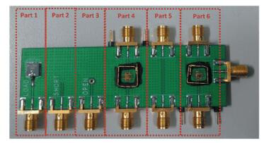
4 Experiment Results Analysis Based on the above theory, the three-level cascade structure model can be treated as a continuous waveguide transfer. The COB board is designed and established as demonstrated in Fig. 4. Table 2 shows the actual experiment plans. Different splits are built in order to do the verification and comparison. The COB is separated into six parts. Parts 1-3 are the load board (LB) CAL kits which include OPEN/SHORT/LOAD. They are used to do load board calibration to de-embedding the trace, welding spot and connector. Part 4 is the COB device under test. Part 5 is the microstrip line trace which combines the Agilent standard CAL kits to de-embedding the thru structure. Part 6 is the microstrip line trace with the direct bonding wire to de-embedding the effect on wire bonding. Moreover, the tester that we do COB verification is Advantest 93K. The platforms that we do on-wafer verification are Cascade Microtech prober and Agilent PNA E8363.
表 2

Table 2 Description on experiment plan
| No |
Split plan |
Used part |
Calibration method description |
| 1 |
LB CAL |
1+2+3+4 |
COB Open/Short/Load to avoid trace affect |
| 2 |
Agilent CAL+Trace |
5+4 |
Equivalent bonding wire as a half trace |
| 3 |
Agilent CAL+Bonding |
6+4 |
Actual bonding wire mode de-embedding |
| 4 |
Agilent CAL |
/ |
Just set the error model plane to the connector |
|
Table 2 Description on experiment plan
|
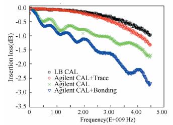
Through the experiments tested, the insertion loss (IL) comparison trend chart is drawn and summarized in Fig. 5. From the test results, we can estimate that LB CAL and Agilent CAL+Trace almost obtain the same results because only trace length is different in 1X or 2X length. However, if the calibration plane is set to SMA connector only, the connectors' loss would be involved in the actual test. The worst case obtained is the Agilent CAL + bonding wire. The bonding wire angle or solder points will affect the results because the bonding wire on the calibration trace may be different from the actual device we tested. It leads to over or under calibration while extended OSL is used to de-embedding.
Since the experimental IC device is the single structure RF switch whose design application is in mobile terminal, the popular cell operation frequency points (CDMA net_800M, GSM net_900M, GSM net_1.8G, 3G net_2.0G, 4G LTE net_2.7G) are selected to do detail analysis. Moreover, on-wafer results tested on Cascade platform with ISS calibration kits are selected as a golden standard. Table 3 shows the calculated results based on Table 4, and we can find max error rate on different de-embedding method will reach 1.319 dB at 2.7 G as shown in Table 3. With the increase of frequency, the errors would be brought more seriously. Therefore, the actual performance of the device is totally submerged in the errors.
表 3

Table 3 Max error analysis on IL comparison
| (dB) |
| Solution |
800M_delta |
900M_delta |
1.8G_delta |
2.0G_delta |
2.7G_delta |
| LB CAL |
-0.001 |
-0.001 |
0.015 |
0.008 |
0.027 |
| Agilent CAL+Trace |
0.002 |
0.006 |
-0.014 |
-0.024 |
-0.057 |
| Agilent CAL |
-0.350 |
-0.461 |
-0.610 |
-0.562 |
-0.692 |
| Agilent CAL+Bonding |
-0.579 |
-0.661 |
-1.051 |
-0.877 |
-1.292 |
| Max Error |
0.581 |
0.667 |
1.066 |
0.885 |
1.319 |
|
Table 3 Max error analysis on IL comparison
|
表 4

Table 4 Insert loss under different frequencies and solutions
| (dB) |
| Solution |
CDWA_800M |
GSM_900M |
GSM_1.8G |
3G_2.0G |
4G_LTE_2.7G |
| LBCAL |
-0.070 |
-0.072 |
-0.144 |
-0.212 |
-0.290 |
| Agilent CAL+Trace |
-0.067 |
-0.065 |
-0.173 |
-0.244 |
-0.374 |
| Agilent CAL |
-0.419 |
-0.532 |
-0.769 |
-0.782 |
-1.009 |
| Agilent CAL+Bonding |
-0.648 |
-0.732 |
-1.210 |
-1.097 |
-1.609 |
| Cascade CP |
-0.069 |
-0.071 |
-0.159 |
-0.220 |
-0.317 |
|
Table 4 Insert loss under different frequencies and solutions
|
As a result, it is clarified that the on-board CAL kits solution is the best way to do the de-embedding on COB test. The on-board CAL kits solution can decrease the system error to the least value that the max error shift can be controlled less than 0.1 dB. What's more, the CAL kits accuracy and CPW structure should be strict controlled or the results will quite be influenced.
5 Conclusions This paper analyzes the system error model and compares the different de-embedding methods through the one-port calibration method (extended OSL). During the analysis, the max error has been controlled in the least level on COB test. The approach not only solves the problem on actual chip calibration plan extension but also improves the distinct ports coverage. However, the on-board CAL kits solution should be accurately monitored to avoid the reflection. In a conclusion, the on-board CAL kits solution is established for the future engineer COB's S parameter verification. And it also generates effective solution to avoid the error model with the testing reference plane shifted. Last but not least, it brings the valuable guide line on COB de-embedding method to get the high accurate and real results.
 2)
2)
 1)
1)
 1)
1)
 1)
1)
 1)
1)
 1)
1)
 1)
1)
 1)
1)
 1)
1)
 1)
1)
 1)
1)
 3)
3)
 1)
1)
 1)
1)
 1)
1)
 1)
1)
 1)
1)
 1)
1)
 1)
1)
 1)
1)
 1)
1)
 2017, Vol. 24


