2. Advanced Innovation Center for Soft Matter, Beijing University of Chemical Technology, Beijing 100029, China
Quantization is a fundamental process in analog to digital converters (ADCs). Emerging wireless standards require the ADCs to possess wide bandwidth, high dynamic range, high signal to noise rate (SNR), simple structure, and low power consumption[1-2]. Sigma-Delta (ΣΔ) ADCs are promising for achieving these features because of their simplified oversampling and noise-shaping features. ΣΔ modulator is the most important part in ΣΔ ADC systems so that high performance ΣΔ modulators are much desired to be researched.
At present, the industrial demand for ΣΔ modulators have been quickly increased since it was successfully used in Micro-Electromechanical System (MEMS) accelerometers[3-6]. Closed-loop ΣΔ modulators enable MEMS accelerometers to effectively suppress the quantization noise caused by ADCs or quantizers[7-10]. Based on these advantages, many researchers have been striving to enhance dynamic range, linearity, and bandwidth of ΣΔ modulators. So far, in order to improve both stability and noise-shaping ability, ΣΔ modulators are always designed by single loop and high-order architectures. Therefore, many latterly reported interfaces for ΣΔ modulators possess the features of single loop, high-order, and single-bit force feedback[11-13]. However, such architecture has to confront with loop instability. Therefore, it is necessary to compromise many aspects in circuit implementation so as to design a high performance ΣΔ modulator system with ideal robust stability. The stability of ΣΔ modulators will be weakened by unavoidable noises including Brownian noise, electrical noise, and quantization noise.In this paper, we applied a novel disturbance observer (DOB) with a Bode's ideal cut-off (BICO) filter to eliminate the system noises for ΣΔ modulators[14]. Specifically, a BICO filter was employed in the DOB to provide disturbance rejection performance for compensating the system noises and modeling mismatches.
In this paper, the proposed BICO with DOB was designed to make up mismatches of system parameters and external disturbances for ΣΔ modulator systems. It is normally impossible to obtain an accurate mathematic model for a ΣΔ modulator because of the Brownian noise, electrical noise, and quantization noise or deviations in the manufacturing process. However, the proposed BICO-DOB applied a fractional-order filter, which can provide extra freedom to improve performance by weakening the effect of system noises[15].
A BICO-DOB for the ΣΔ modulator was used in this paper. The rest of the paper is structured as follows: Section 2 demonstrates the concept of BICO-DOB and Section 3 presents the proposed BICO-DOB for the ΣΔ modulator. Then simulation results from the proposed high-order ΣΔ modulator with BICO is given in Section 4 with the conclusions drawn in Section 5.
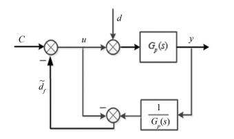
2 Disturbance ObserverThe simplified architecture of a DOB is depicted in Fig. 1.
|
Fig.1 Simplified architecture of a DOB |
In Fig. 1, Gp(s) denotes the plant model, d and
| $ \tilde{d}_{f}=(u+d) \cdot G_{p}(s) \cdot G_{p}^{-1}(s)-u=d $ | (1) |
According to Eq. (1), the equivalent disturbance d is well observed by the DOB scheme shown in Fig. 1. DOB can also achieve independent tuning between the disturbance elimination and input command under the condition of external disturbances and modelling deviations. However, the realization of a DOB suffers three problems in a certain system[16] as follows:
1) Under normal conditions, the numerator's order of Gp(s) is less than or equal to the denominator's order so that Gp-1(s) cannot be implemented in practical systems;
2) The mathematic model Gp(s) is inaccurate due to the parameters' variation caused by external or internal disturbances;
3) The control quality of a practical system would be deteriorated by the unavoidable noises.
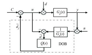
Fortunately, a Q-filter and Gn(s) can be used to solve the abovementioned problems. Fig. 2 depicts the modified structure of the DOB.
|
Fig.2 Modified structure of the DOB |
In Fig. 2, Q(s) is used to realize the Gp-1(s)·Q(s) and the Q-filter can be expressed as
| $ Q(s)=\frac{1}{(\tau s+1)^{n}} $ | (2) |
where τ is a time constant, n is the order, which is selected to make Gp-1(s)·Q(s) realizable. In other words, n is selected to make the numerator's order of Gp-1(s)·Q(s) less than or equal to denominator's order. Details about the BICO-DOB are discussed below.
In Ref. [12], the concept of the BICO filter was introduced by Bode, which provides an ideal trade-off between the system phase margin and the cut-off frequency. The BICO filter is expressed by Eq. (3):
| $ \beta(s)=\frac{K}{\left(\sqrt{1+\left(s / \omega_{0}\right)^{2}}+\left(s / \omega_{0}\right)\right)^{2(1-\eta)}} $ | (3) |
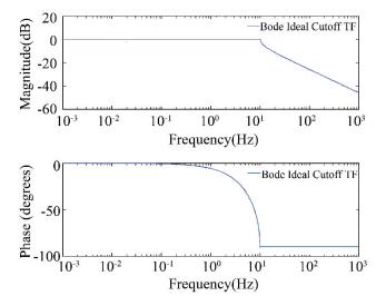
where ω0 denotes cut-off frequency, η is the order of the BICO filter, and η∈(0, 1) is a fractional order. BICO-DOB is provided with more flexibility than the traditional DOB for disturbance elimination. According to Eq. (3), the slope of the β(s) gain is -40(1-η) dB/dec. The Bode plot of β(s) (with ω0=10 and η=0.5) is shown in Fig. 3.
|
Fig.3 Bode plot of the BICO filter |
In this paper, the main topic is to validate the effect of using BICO-DOB scheme on ΣΔ modulators. As is well known, robustness is a crucial aspect to be considered when designing a ΣΔ modulator. As shown in Fig. 3, we can easily find that the BICO filter possesses insensitivity in pass-band frequency range and a sharp cut-off. Also it can be found that the phase of the BICO filter is relatively insensitive to uncertainties in stop-band frequency range because the phase property is almost constant. Therefore, we investigated the validity of applying BICO-DOB motivated by finding an effective way to design high performance and strong robust ΔΣ modulator systems.
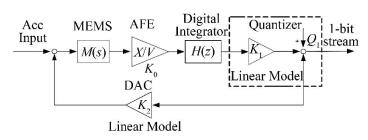
3 High-Order ΣΔ Modulator with BICO-DOBThe basic structure of the ΣΔ modulator is depicted in Fig. 4.
|
Fig.4 Basic structure of the ΣΔ modulator |
As shown in Fig. 4, the high-order ΣΔ modulator consists of six basic functional blocks: a) a mechanical sensor element; b) an AFE block; c) an n-bit ADC; d) a digital loop filter; e) a 1-bit quantizer; and f) a 1-bit DAC. ΣΔ modulator is a mixed nonlinear feedback system made up of components in both mechanical domain and electrical domain.
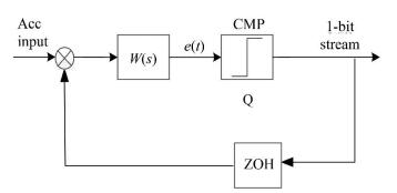
Fig. 5 shows a simplified architecture of the ΣΔ modulator system, where
|
Fig.5 A simplified architecture of the ΣΔ modulator |
In Fig. 5,
| $ W{\rm{ (}}s{\rm{) = }}{K_{\rm{0}}}M{\rm{ (}}s{\rm{) }}H{\rm{ (}}s{\rm{)}} $ | (4) |
where H(s) is the continuous time response of loop filter H(z). The transfer function of the mechanical sensor element M (s) is expressed by Eq. (5):
| $ M(s)=\frac{1}{s^{2}+\frac{b}{m} s+\frac{k}{m}} $ | (5) |
where m, b, and k are the proof mass, damping coefficient, and spring constant, respectively. b and k are not always the certain parameters, which is caused by the manufacturing process.
The proposed structure of the ΣΔ modulator with a BICO-DOB is shown in Fig. 6.

|
Fig.6 Principle of the proposed ΣΔ modulator |
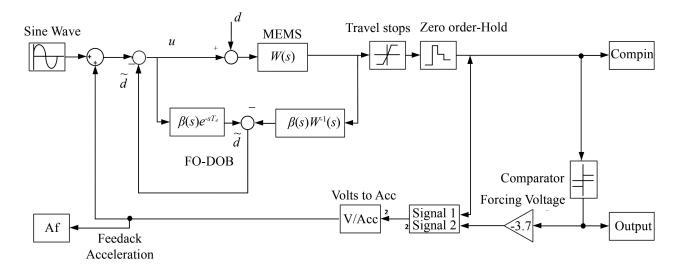
In Fig. 6, W-1(s) is the inverse model of the W(s), β(s) is the BICO filter, and e-s·Td is the time delay. As mentioned above, Brownian noise, electrical noise, and quantization noise are the main noise sources in ΣΔ modulator systems. Brownian noise is caused by thermal motion of the air molecules surrounding the sensor element, and electrical noise is caused by amplifier circuit (AFE), whereas quantization noise comes from the 1-bit quantizer, which can be effectively eliminated by the digital loop filter H(z). In this paper, the BICO-DOB is used to eliminate the effect of the parameters' derivation and the system noise
| $ d_{\text {total }}\left(d_{\text {total }}=d_{\text {Brown }}+d_{\text {Electrical }}\right) $ |
The simulated model of the proposed ΣΔ modulator is shown in Fig. 7.
|
Fig.7 Simulated model of the proposed ΣΔ modulator |
In Fig. 7, the sample frequency is chosen as 128 kHz and the oversampling ratio is specified as 64. The system parameters in Fig. 7 are listed in Table 1.
| Table 1 Parameters of the proposed ΣΔ modulator |
In this paper, we selected a 4th-order filter as the digital loop filter H(z), which can be written as
| $ H(z)=\frac{37 z^{4}-137.1 z^{3}+191.3 z^{2}-119 z+27.86}{z^{4}-2.995 z^{3}+2.99 z^{2}-0.995 z} $ | (6) |
The parameters of the digital loop filter H(z) have been adjusted empirically in our previous experimental work. Thus, we mainly focused on the validity of applying BICO-DOB in ΣΔ modulator systems in this paper, and the design method of parameters of digital loop filter H(z) is not specifically described here. The time delay of the W(s) was about 0.1 ms, so the Td in Fig. 7 was set as 0.1 ms. The cut-off frequency ω0 was set as 1 000 rad/s, and without loss of generality, the gain K of BICO filter β(s) was set as 1.
Therefore, the relative order η of β(s) was the only knob to tune. In order to rapidly obtain and optimize the relative order η, PSO algorithm[17] was applied. In this paper, the SNR was set as the objective of the ΣΔ modulator system, which can be calculated based on the power spectral density of the output bitstream produced by the proposed ΣΔ modulator.
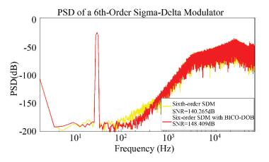
In the numerical experiment, the proposed ΣΔ modulator with BICO-DOB achieved the highest SNR=148.409 dB of SNR by yielding the optimal value for η=-0.25. Therefore, here we took η=-0.25 in Eq. (3):
| $ \begin{array}{c} \beta(s)=\frac{1}{(\sqrt{1+(s / 1000)^{2}}+(s / 1000))^{2.5}}= \\ \frac{1}{(\sqrt{1+(s / 1000)^{2}+(s / 1000)})^{2}} \\ \frac{1}{(\sqrt{1+(s / 1000)^{2}+(s / 1000)})^{0.5}} \end{array} $ | (7) |
It is worth noting that in the simulation the fractional order differentiator s0.5 of the system was approximated with Oustaloup approximation[18] in the frequency range [10-4, 104] rad/s and N=5.
Taking η=-0.25 into Fig. 7 and running the Simulink model (Fig. 7) again, the corresponding SNR was 148.409 dB. Fig. 8 shows the noise floor of the ΣΔ modulator without the BICO scheme. Compared with the ΣΔ modulator without the BICO scheme, the proposed ΣΔ modulator with the BICO-DOB achieved higher SNR and lower noise floor.
|
Fig.8 Noise floor of the proposed ΣΔ modulator |
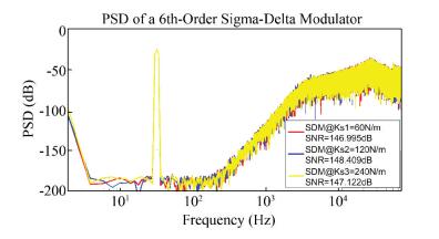
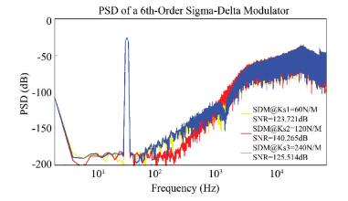
As discussed above, the damping coefficient b and spring constant k are variables all the time. Therefore, we chose different b and k values to verify the robustness of the proposed method. To be specific, we took spring constant as ks1=60, 120, and 240 N/m. Fig. 9 shows the PSD plot of the ΣΔ modulator with different spring constant k values.
|
Fig.9 Noise floor of the ΣΔ modulator with different spring constant k values |
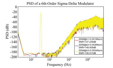
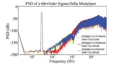
Similarly, we chose different damping coefficient b values to verify the robustness of the proposed ΣΔ modulator. To be specific, we set the b values as 1.8×10⁻³ Ns/m, 3.6×10⁻³ Ns/m, and 5.4×10⁻³ Ns/m. Fig. 10 shows the PSD plot of the ΣΔ modulator with different b values.
|
Fig.10 PSD of the ΔΣ modulator with different b values |
Fig. 11 and Fig. 12 demonstrate the weak robustness of the ΣΔ modulator without the BICO-DOB scheme, which proves that the proposed method possesses better robustness than the pure 6th-order ΣΔ modulator does.
|
Fig.11 Noise floor of the 6th-order ΣΔ modulator with different k values |
|
Fig.12 Noise floor of the 6th-order ΣΔ modulator with different b values |
It can be seen from Figs. 9-12 that the proposed ΣΔ modulator only shows slight fluctuation in noise floor and SNR, which indicates that the proposed BICO-DOB scheme enables the ΣΔ modulator to be robust to the variable parameters of the sensor element. We can also find that the robustness of the proposed ΣΔ modulator is stronger than the pure 6th-order ΣΔ modulator.
5 ConclusionsA new design of a 6 th-order ΣΔ modulator using the proposed BICO-DOB is presented in this paper. The designed 6 th-order ΣΔ modulator achieved SNR=148.409 dB and noise floor under -190 dB in the simulation study. The results from the simulation by MATLAB platform show that the proposed BICO-DOB scheme for the ΣΔ modulator can achieve better robustness.
| [1] |
Qian L, Bi Z, Zhou D, et al. Automated technology migration methodology for mixed-signal circuit based on multistart optimization framework. IEEE Transactions on Very Large Scale Integration (VLSI) Systems, 2015, 23(11): 2595-2605. DOI:10.1109/TVLSI.2014.2377013 (  0) 0) |
| [2] |
Bafandeh A, Yavari M. Digital calibration of amplifier finite DC gain and gain bandwidth in MASH ΣΔ modulators. IEEE Trans. Circuits and Systems Ⅱ: Express Briefs, 2016, 63(4): 321-325. DOI:10.1109/TCSⅡ.2015.2504027 (  0) 0) |
| [3] |
Marek J. MEMS for automotive and consumer electronics. Digest of Technical Papers - IEEE International Solid-State Circuits Conference, 2010, 53: 9-17. DOI:10.1109/ISSCC.2010.5434066 (  0) 0) |
| [4] |
Xu Honglin, Liu Xiaowei, Fu Qiang, et al. A high-order closed-loop ΣΔ interface for micro-machined accelerometer sensor. Analog Integrated Circuits and Signal Processing, 2015, 82(2): 401-410. DOI:10.1007/s10470-014-0436-4 (  0) 0) |
| [5] |
Schmid H, Sigel S, Pastre M, et al. An internally non-linear ADC for a delta-sigma accelerometer loop. International Symposium on Circuits and Systems Nano-Bio Circuit Fabrics and Systems. Paris, 2010, 2155-2158. (  0) 0) |
| [6] |
Petkov V P, Boser B. High-order electromechanical ΣΔ modulation in micromachined inertial sensors. IEEE Trans. Circuit and Systems I: Regular Papers, 2006, 53(5): 1016-1022. DOI:10.1109/TCSI.2006.869901 (  0) 0) |
| [7] |
Briseno-Vidrios C, Edward A, Shafik A, et al. A 75 MHz BW 68 dB DR CT-ΣΔ modulator with single amplifier biquad filter and a broadband low-power common-gate summing technique. In Proc. Symp. VLSI Circuits (VLSI Circuits), Piscataway: IEEE, 2015. C254-C255. DOI: 10.1109/VLSIC.2015.7231277.
(  0) 0) |
| [8] |
Andersson M, Anderson M, Sundstrom L, et al. A filtering ΣΔ ADC for LTE and beyond. IEEE J. Solid-State Circuits, 2014, 49(7): 1535-1547. DOI:10.1109/JSSC.2014.2319254 (  0) 0) |
| [9] |
Kauffman J G, Witte P, Lehmann M, et al. A 72 dB DR, CT ΣΔ modulator using digitally estimated, auxiliary DAC linearization achieving 88 fJ/conv-step in a 25 MHz BW. IEEE J. Solid-State Circuits, 2014, 49(2): 392-404. DOI: 10.1109/JSSC.2013.2289887.
(  0) 0) |
| [10] |
Weng C H, Wei T A, Alpman E, et al. A continuous-time delta-sigma modulator using ELD-compensation embedded SAB and DWA-inherent time-domain quantizer. IEEE J. Solid-State Circuits, 2010, 51(5): 1235-1245. DOI:10.1109/JSSC.2016.2532345 (  0) 0) |
| [11] |
Lu C Y, Onabajo M, Gadde V, et al. A 25 MHz bandwidth 5th-order continuous-time low-pass sigma-delta modulator with 67.7 dB SNDR using time-domain quantization and feedback. IEEE J. Solid-State Circuits, 2010, 45(9): 1795-1808. DOI:10.1109/JSSC.2010.2050942 (  0) 0) |
| [12] |
Srinivasan V, Wang V, Satarzadeh P, et al. A 20 mW 61 dB SNDR (60 MHz BW) 1b 3rd-order continuous-time delta-sigma modulator clocked at 6 GHz in 45 nm CMOS. In IEEE Int. Solid-State Circuits Conf. Dig. Tech. Papers (ISSCC). Piscataway: IEEE, 2012. 158-160.
(  0) 0) |
| [13] |
Long S, Liu Y, He K, et al. 116 dB dynamic range CMOS readout circuit for MEMS capacitive accelerometer. Journal of Semiconductors, 2014, 35(9): 1-5. (  0) 0) |
| [14] |
Bode H W. Network Analysis and Feedback Amplifier Design. New York: R. E. Krieger Pub. Co, 1945.
(  0) 0) |
| [15] |
Olivier L E, Craig I K, Chen Y Q. Fractional order and BICO disturbance observers for a run-of-mine ore milling circuit. Journal of Process Control, 2012, 22(1): 3-10. (  0) 0) |
| [16] |
Wei Jiaqing. Disturbance rejection through disturbance observer with adaptive frequency estimation. IEEE Transactions on Magnetics, 2009, 45(6): 2675-2688. DOI:10.1109/TMAG.2009.2018605 (  0) 0) |
| [17] |
Kennedy J, Eberhart R. Particle swarm optimization. IEEE Conf. Neural Networks, Perth. Piscataway: IEEE, 1995. 1942-1948.
(  0) 0) |
| [18] |
Oustaloup A, Levron F, Mathieu B, et al. Frequency-band complex noninteger differentiator: Characterization and synthesis. IEEE Trans. Circuit Syst. I: Fundamental Theory and Applications, 2000, 47(1): 25-39. DOI:10.1109/81.817385 (  0) 0) |
 2020, Vol. 27


