The scaling of transistor size has been the fundamental driver of the exponential advances in integrated circuit performance that have occurred over the last three decades. The intrinsic advantages of MOSFET scaling include speed improvement and energy reduction. The benefits of MOSFET scaling declined when the technology node was scaled below 45 nm due to the emergence of quantum effects. Since low-dimensional CMOS devices are widely used in both digital and analogue circuits, it is necessary to accurately characterize quantum effects in order to achieve high performance in the design of nanoscale circuits[1-3]. Obtaining closed-form analytical models for nanodevices is challenging or almost impossible in the context of analytical modelling due to the complexity involved in VLSI design at an ultradeep submicron technology node. As a result, models are constructed by simplifying the complete physical model. The compact models make it possible to simulate nanoscale circuits at the system level in a short amount of time. However, due to the simplifications performed during the model creation process, the accuracy of such a model might be less. When designing complicated systems, accuracy and simplicity of models are critical considerations. A model based on artificial intelligence would be preferable, since it would be more realistic and deliver practical solutions[4-7].
Ref.[8] presented CMOS based inverter design considering propagation delay and using an artificial bee colony optimization algorithm. Refs.[9] and [10] investigated the switching characteristics of a CMOS inverter using neural networks and particle swarm optimization techniques, demonstrating the utility of ANN in solving complex nonlinear problems. Ref.[11] designed a three-phase photovoltaic grid linked inverter using a radial basis function neural network, and Ref.[12] designed a cascaded H-Bridge multilevel inverter using a Neural Network controller. Ref.[13] presented a summary of the diverse fields in which neural networks can be applied. In all the above work, long channel equations have been taken into consideration for predicting delays, which cannot be used for lower technology nodes. Thus, in this work, α-power law based approximate delay model has been taken into account for predicting delays at up to an ultradeep submicron technology up to 22 nm.
CMOS inverter is generally considered to be the fundamental part of any digital circuit. Its design is very crucial in the development of digital integrated circuits[13]. If we are moving towards the nanoscale regime, modelling device behaviour with advanced methodologies becomes of utmost importance since the problem becomes more complicated with the large number of parameters involved and cannot be modelled using simple equations[14]. This paper explores the technique of building a CMOS inverter with an artificial neural network having several hidden layers at different technology nodes and different temperatures. I have examined how well my proposed model[15] can be extended to predict the delay of a CMOS inverter at a given technology node and operating temperature. The aspect ratio, load capacitance, and supply voltage are the three parameters taken as ANN input parameters. The aim is to describe the problem statement, the input and output parameters of ANN, its configuration, and the outcome of various experiments performed. The following are the four important contributions:
1) Using the unified and approximate drain current approach based on the α-power law-based model for strong, moderate, and weak inversion regions described in my earlier work[15], the delay of the CMOS inverter is estimated. The results obtained for drain current in Ref.[15] were in proximity with HSPICE within the acceptable error range of 0-2%. Table 1 represents the values of the model parameters taken into consideration which was extracted using HSPICE simulation utilizing predictive technological model (PTM) [16].
| Table 1 Obtained values of α, I0 and Vth at different temperatures and technology nodes |
2) Velocity saturation index α, specific current I0 and threshold voltage Vth are the temperature-dependent parameters in the proposed delay equation. The variance of these temperature-dependent parameters has been demonstrated, and the curve has been modified to simpler quadratic equations.
3) The applicability of ANN in the design of microelectronic circuits at an ultradeep submicron technology node is discussed in this work. Because of this, an inverter structure has been used to show the algorithms, taking into account their dynamic properties.
4) For the NOT gate, an ANN network has been constructed that approximates the rise time in response to varying input voltage levels, load capacitance, and aspect ratio. The methodology has been adopted for the temperature range of 300 K-400 K to validate our models against analytical data and HSPICE simulations.
The following is the procedure adopted:
1) First, in order to set the input layer of the neural network, data sets were created by HSPICE simulation and mapped to some random functions and the proposed model (Refer to Table 2) in order to remove the biasness of the data. Further, training and testing methods were adopted which provided encouraging and successful results at technological nodes ranging from 130 nm to 22 nm and temperatures ranging from 298.15 K to 398.15 K. Thus, the structure can be used to generate and predict additional outputs for a variety of different input values.
| Table 2 Amount of time required to calculate the ANN model for various functions |
2) The improvement in the simulation speed of ANN over HSPICE was observed and tabulated in Table 3. It shows that the ANN model is very accurate and that its simulation is much quicker than that of the HSPICE. Thus, these blocks may be used in conjunction with software tools such as PSPICE or alone as a simulator for the design and modelling of CMOS logic circuits.
| Table 3 Speed improvement comparison of HSPICE and ANN |
1 Introduction to Neural Networks
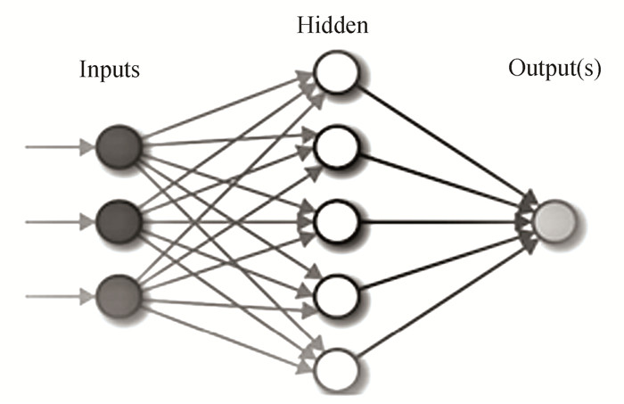
Modeling complicated and nonlinear processes using artificial neural networks (ANNs) has become more popular in recent years. A hidden-layer artificial neural network connects a problem's input and output patterns. In these networks, communication links are weighted, as shown in Fig. 1. Learning algorithm sets weights. Output for hidden layer node j:
|
Fig.1 ANN structure |
| $ h_j=g\left(\sum\limits_{i=1}^n w_{i j} \cdot x_i+b_j\right) $ | (1) |
The network output is given as:
| $ y=\sum\limits_{i=1}^k w o_i \cdot h_i $ | (2) |
where wij are the input weights to node j of the hidden layer, bj is the node bias, and woi are the hidden-to-output weights.
ANNs may be categorized by their learning algorithm: ANNs with set weights do not require learning[17-18]. Unsupervised ANNs: Their weights are solely updated based on input data. The networks adapt based on previous input. Most ANNs are supervised. Both input and output network data are used.
The activation function determines a neuron's output and input based on its input activity. Threshold, piecewise linear, sigmoid, tangent hyperbolic, and Gaussian are common functions[17]. The network calculates weights and biases by analyzing input-output data. Back-propagation is one approach to get these characteristics[17-19]. Weights and biases are changed periodically to reduce the network's mean square error. This approach may be used incrementally or batch-wise. After each input, weights and biases are modified progressively. In batch mode, weights and biases are modified after the whole training set.
In this paper, the ANN architecture used has been designed by mapping design parameters to CMOS inverter output parameters for a given process technology. Further, the model was extended to see if it could handle the effect of rising temperature. The dataset utilized to train the model was obtained from the proposed analytical model and divided into two sets: (1) Inverter delay at room temperature at 300 K for different load capacitance, supply voltage and aspect ratio. (2) Inverter delay at elevated temperature of 400 K for different load capacitance, supply voltage and aspect ratio.
The number of input nodes of a neural network is chosen as per our choice of mapping variables to the desired output. To improve the accuracy of the ANN, the number of hidden layers, the number of units present in the hidden layer, activation function and the other parameters should be properly chosen. The neural network used in this paper has three inputs: Wn/Wp ratio, load capacitance and supply voltage. The output parameter is delay (rise time). The training was done with 70 % data, validation with 15 % data and testing was done with the remaining 15% data.
2 α-power Law Based CMOS Delay ModelThe speed of digital systems is affected by the way digital integrated circuits switch. A digital system's transient performance requirements are typically among the most critical design specifications that the circuit designer must fulfill. It is important to estimate and optimize the circuit's switching speed early in design[20]. The closed-form time delay functions were extracted under the presumption of pulse excitations for lumped load capacitance. When Vgs=Vds=Vdd, the ON current of MOSFET, ION, can be expressed as[15]:
| $ I_{\mathrm{ON}}=I_0 \ln ^\alpha\left[1+\exp \left(\frac{V_{\mathrm{dd}}-V_{\mathrm{th}}}{2 n \phi_t}\right)\right] $ | (3) |
Here,
The CMOS inverter's time delay is calculated by the time it takes to charge or discharge the load. The delay of propagation, tp, of a gate can be represented as:
| $ t_p=\frac{C_L V_{\mathrm{dd}}}{I_{\mathrm{ON}}} $ | (4) |
Here, CL is the output load capacitance; ION is the ON current of MOSFET on drain.
Substituting the value of ION from Eq.(3).
| $ t_p=\frac{C_L V_{\mathrm{dd}}}{2 n \mu_{\mathrm{eff}} C_{o x} \frac{W}{L} \phi_t^2} \cdot \frac{1}{\mathrm{IC}} $ | (5) |
Here,
| $ \mathrm{IC}=\ln ^\alpha\left[1+\exp \left(\frac{V_{\mathrm{dd}}-V_{\mathrm{th}}}{2 n \phi_t}\right)\right] $ | (6) |
Load capacitance CL is the amount of the intrinsic capacitance of the fan-out gates from the driving phase and is thus proportional to:
| $ C_L \propto C_{o x} L\left(\xi_i W_i+W_{i+1}\right) $ | (7) |
where ξi is the ratio of driver-stage parasitic capacitance to fanout-stage input gate capacitance. Driver and load stage annotations are i and i+1. In Eq. (5), W becomes Wi. Putting CL from Eq. (7) into Eq. (5),
| $ t_p=\frac{L^2}{2 n \mu_{\mathrm{eff}} \phi_t^2} \cdot \frac{V_{\mathrm{dd}}}{\mathrm{IC}} \cdot \frac{\xi_i W_i+W_{i+1}}{W_i} $ | (8) |
For N numbers of stages across the pathway, the path delay can be estimated as sum of the gate delays. Thus,
| $ \mathrm{PD}=\frac{L^2}{2 n \mu_{\mathrm{eff}} \phi_t{ }^2} \cdot \frac{V_{\mathrm{dd}}}{\mathrm{IC}} \sum\limits_{i=1}^N \frac{\xi_i W_i+W_{i+1}}{W_i} $ | (9) |
| $ \mathrm{PD}=k_{\mathrm{pd}} \frac{V_{\mathrm{dd}}}{\mathrm{IC}} \mathrm{PD}(W) $ | (10) |
where kpd is a technology-dependent factor, and PD(W) relies on the path transistor's gate size. Traditional latency for N stages may be described in terms of the average single-stage propagation delay tp and the logic depth Ld, but this does not enable gate sizing.
| $ P D=t_{\mathrm{p}} L_{\mathrm{d}} $ |
I0, Vth, ϕt and α are the temperature-dependent system parameters that differ with respect to temperature in Eq. (5). One of the most powerful temperature dependent functions is the threshold voltage. The threshold voltage dependence on temperature can be expressed as[21]:
| $ \mathrm{NMOS} \\ \,\,\,\,\,\,\,\,\,\, V_{\mathrm{th}}(T)=V_{\mathrm{th}}\left(T_0\right)+\alpha_T\left(\frac{T}{T_0}-1\right) $ | (11) |
| $ \mathrm{PMOS} \\ \,\,\,\,\,\,\,\,\,\, V_{\mathrm{th}}(T)=V_{\mathrm{th}}\left(T_0\right)-\alpha_T\left(\frac{T}{T_0}-1\right) $ | (12) |
Here Vth(T0) is the threshold voltage obtained at the room temperature; αT is the temperature coefficient of device threshold voltage.
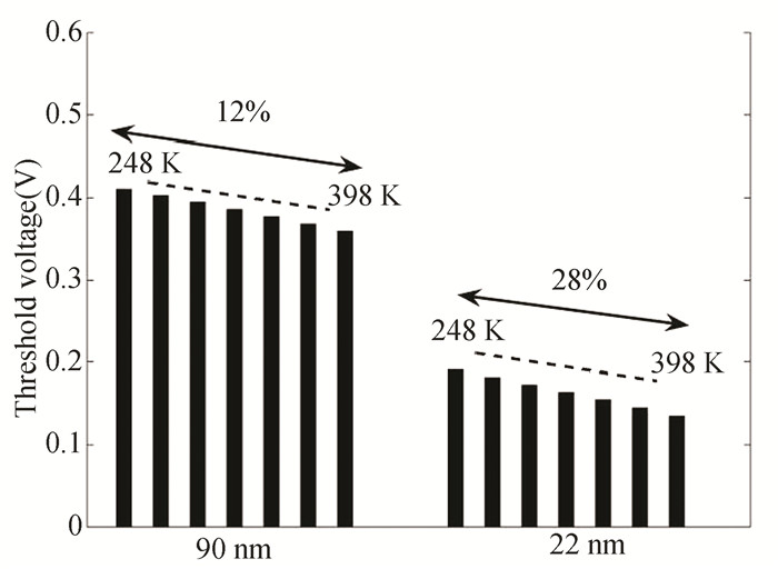
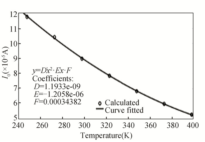
Fig. 2 illustrates the threshold voltage at 90 nm and 22 nm (see Table 1 for 130 nm to 22 nm). The figure shows that a smaller technology node has more variability in temperature-based threshold voltage. Today's manufacturing technique introduces a limited quantity of high-energy dopant atoms into silicon. Each system's dopant atom placement and distribution cannot be properly regulated. Dopant concentration affects threshold voltage[22]. Through HSPICE simulation, extracted parameter αT measures threshold voltage variation. Next, temperature affects I0 current. In the I0 equation, μeff and ϕt are temperature-varying factors. The temperature-dependent specific current I0 at 32 nm is depicted in Fig. 3. The plotted curve is a quadratic expression.
|
Fig.2 Percentage difference in NMOSFET threshold voltage with respect to the change of two nodes of the technology(Vdd=1 V) |
|
Fig.3 Curve fitting plot at 32 nm technology node with specific current changing with temperature(Vdd=1 V) |
| $ I_0(T)=D(T)^2+E(T)+F $ | (13) |
The technology dependent fitting parameters obtained using the Levenberg-Marquardt algorithm here are D, E and F.
The Velocity Saturation Factor α is the next parameter that varies with temperature. By equating the transistor ON current provided in Eq.(3) with that obtained via HSPICE simulation, the values of α at different temperatures are computed.
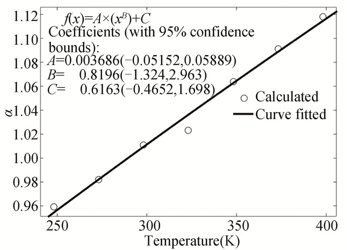
The temperature variation of α is tabulated in the Table 1 from 130 nm-22 nm technology node. Fig. 4 shows the variance of α with respect to the 32 nm technology node temperature. With the following curve-fitted expression, it can be better described.
|
Fig.4 Curve fitted the velocity saturation index α plot with 32 nm node technology temperature(Vdd=1 V) |
| $ \alpha(T)=A(T)^B+C $ | (14) |
The technology-dependent fitting parameters acquired using the Levenberg-Marquardt algorithm are A, B, C here. For further study of the circuit output at different temperatures, the temperature-based expressions for Vth, I0 and α can be used. From the above graphs, it can be concluded that the value of threshold voltage decreases as temperature rises, α increases and I0 decreases.
4 Design of CMOS Inverter using ANNMoore's law has sustained the global semiconductor industry for four decades. However, as we enter the era of nanoscale technologies, scaling-as-usual faces substantial challenges[23]. Naturally, the issues are well-known. Simple scaling eventually ceases to exist as we approach greater atomistic dimensions. Although the devices are smaller, several performance characteristics deteriorate: leakage increases, gain declines, and susceptibility to inevitable tiny manufacturing process changes increases considerably. Many modern designs are constrained by power and energy constraints. We can no longer anticipate worst-case behavior for these technologies based on experience with a few process corners. Nothing is deterministic anymore: the majority of critical factors are statistical in nature; many displays intricate relationships and distressingly large variations. The increasing costs of producing circuits in these scaled technologies (e.g., mask prices) aggravate these predictability issues[24]. Nonetheless, we see substantial opportunity in these difficulties. The purpose of this study is to provide a solution by taking advantage of ANN by analyzing how circuits are designed and effectively respond when such problems arise. Given space limitations, we restrict our focus to the design and analysis of the CMOS inverter.
The neural network presented in this paper for designing a CMOS inverter has three hidden layers with sizes of 20, 10, and 8 (Refer to Fig. 5). In this article, the fitnet MATLAB command is used to generate the fitness function of the neural network. The training of the network is done by Bayesian Regularization Backpropagation[25]. Bayesian Regularization is generally used to minimize a linear combination of squared errors and weights. Moreover, it also modifies the linear combination which results in a network with strong properties of generalization at the end of training. Matlab has a Trainbr network training function that is based on LM (Levenberg-Marquardt) optimization to change the weight and the bias values. Trainbr's default parameters have been utilized in the present work.

|
Fig.5 ANN structure |
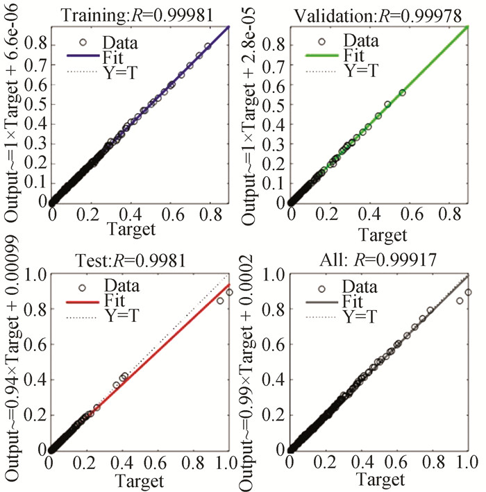
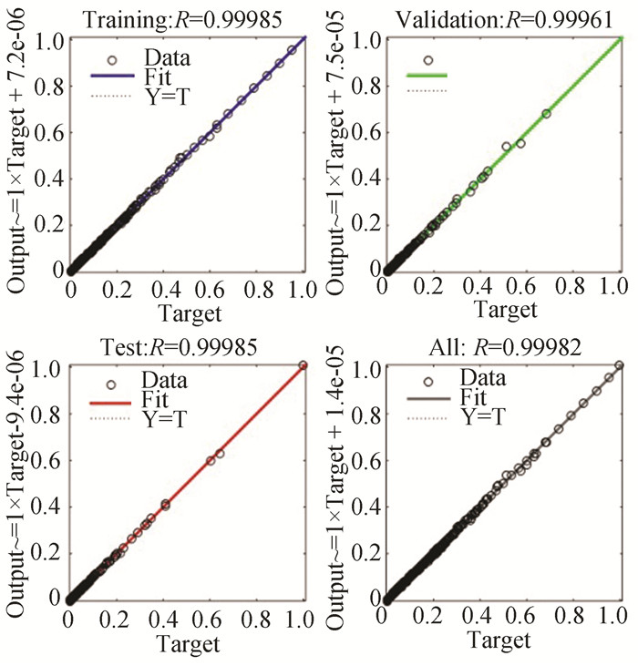
A statistical model's ability to accurately predict a result is measured by a value known as the coefficient of determination (R), which may range from 0 to 1. The R may be interpreted as the percentage of variance in the dependent variable that is predicted by the statistical model. The accuracy of the proposed analytical model can be predicted as the coefficient of determination (R) as described in the accuracy plots of 130 nm and 22 nm technologies at two different temperatures (298.15 K and 398.15 K) in this paper.
5 Results and DiscussionTo begin, it is necessary to decide on a development environment in which the neural model should be built and then eventually implemented. As a result, MATLAB has been chosen to be the tool of choice for designing and developing the necessary neural network models. The neural network is constructed by first producing the appropriate programme code in the MATLAB console, which is followed by decorating the code with the appropriate algorithms and necessary specifications. The Neural Network model was made to make things more accurate. It has more hidden layers than other models and is used to measure quality.
Next step is to pick training and testing data sets from the data obtained from HSPICE simulation. By cutting the full data set into two halves with suitable index mapping, 70 % of it is used for training and the rest for testing. The training data set is used to teach the neural network what to do, and the test data set is used to see how well it did. Next, the trained neural network was tested. The training dataset's lowest and maximum values are used to train the neural network for improved performance.
The least-squares support-vector machine (LSSVM) is an effective technique to effectively scale the larger data-set available in the literature for statistics and statistical modelling. It is the least-squares versions of support-vector machines. SVMs are a set of related supervised learning methods that analyze data and recognize patterns, and they are used for classification and regression analysis. In LSSVM, the answer is obtained by solving a series of linear equations, as opposed to the convex quadratic programming (QP) problem that is required for standard support vector machines (SVMs)[26-28]. The same can be used for scaling effectively the larger data as my future work.
Next, the training process is conducted by giving the correct training function and parameters for the specific problem set and the parameters of the neural network, i.e., proper algorithm, number of neurons, number of layers, number of hidden layers, etc. For iterative estimates and improved performance, the neural network is initialized using the specified parameters. Checking neural network training results may reduce the network's mistake rate. Choosing the right training algorithm maximizes neural network training time. Table 2 shows the mean square error computed as described below and the CPU time required for different functions:
| $ \frac{1}{n} \sum\limits_{i=1}^n\left[\frac{\text { Actual }- \text { Simulated }}{\text { Actual }}\right] \times 100 $ | (15) |
After seeing the results obtained from the proposed model as described in Table 2, following methodology was adopted for further analysis:
1) The ANN model is trained for a single inverter from the delay obtained from the analytical model (Eq.(8)) at room temperature of 300 K and at temperature of 400 K.
2) Eq. (8) is utilized to seed a dataset of 2000 points for 22 nm technology node and 5000 points for 130 nm technology node. The variation of load capacitance, supply voltage and Wn/Wp ratio were taken into consideration while building up the dataset.
3) Table 1 contains the values of α, I0 and Vth at different temperatures and technology nodes used in the analytical model given in Eq. (8). It is important to note that when measuring delays in this paper, input rise time has been kept negligible.
4) The mean squared error measures the average of the squares of the errors—that is, the average squared difference between the estimated values and the actual value. The performance is predicted by Eq.(15).
a) Fig. 5 presents the structure of the neural network that was used in this paper. All sections of the analysis described in Section 1 were conditioned on the same ANN hardware for different datasets with the main exception being the number of epochs.
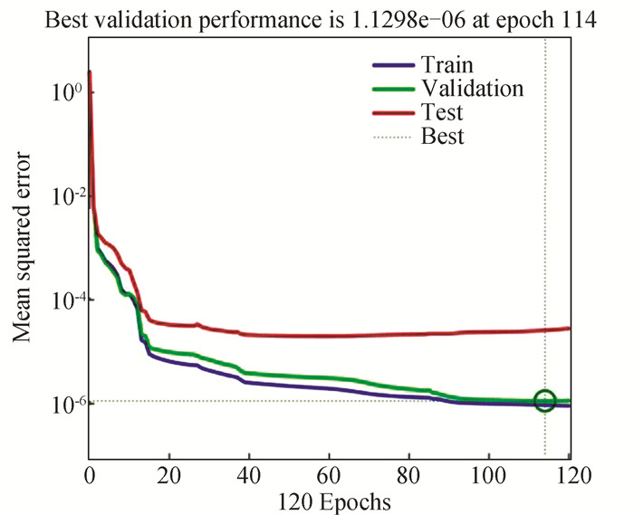
b) Fig. 6 and Fig. 7 show the performance and the accuracy plots respectively for the ANN model at 22 nm technology node (300 K).
|
Fig.6 Performance plot of analytical model at 22 nm technology node (room temperature) |
|
Fig.7 Accuracy plot of analytical model at 22 nm technology node (room temperature) |
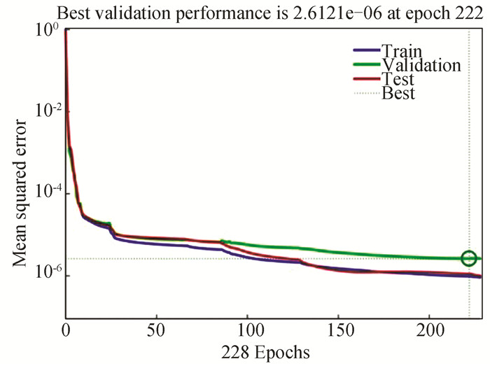
c) Fig. 8 and Fig. 9 show the performance and the accuracy plots respectively for the ANN model at 22 nm technology node (400 K).
|
Fig.8 Performance plot of analytical model at 22 nm technology node (398.15 K) |
|
Fig.9 Accuracy plot of analytical model at 22 nm technology node (398.15 K) |
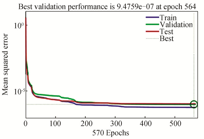
d) Fig. 10 and Fig. 11 show the performance and the accuracy plots respectively for the ANN model at 130 nm technology node (300 K).
|
Fig.10 Performance plot of analytical model at 130 nm technology node(room temperature) |

|
Fig.11 Accuracy plot of analytical model at 130 nm technology node (room temperature) |
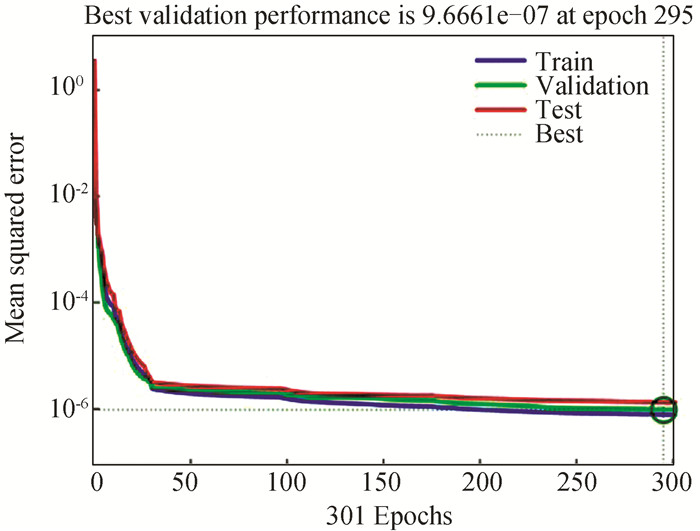
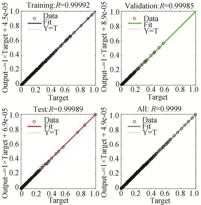
e) Fig. 12 and Fig. 13 show the performance and the accuracy plots respectively for the ANN model at 130nm technology node (400K).
|
Fig.12 Performance plot of analytical model at 130 nm technology node (398.15 K) |
|
Fig.13 Accuracy plot of analytical model at 130 nm technology node (398.15 K) |
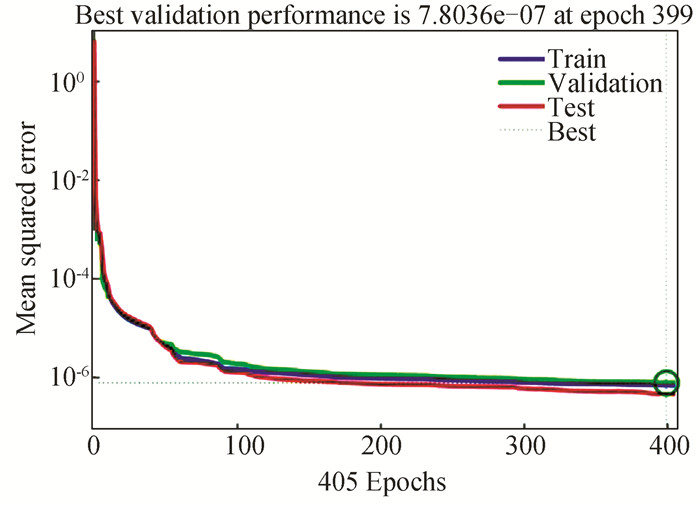
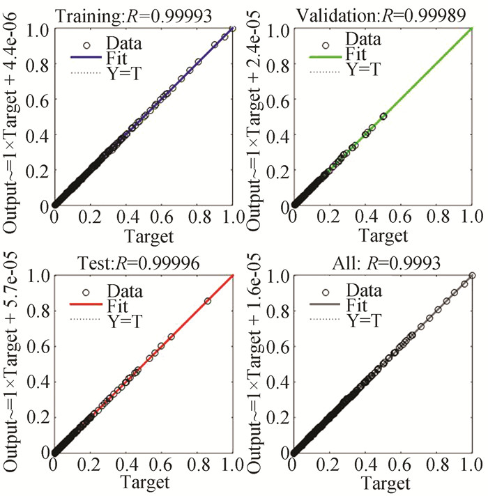
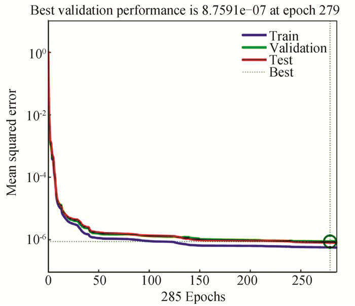
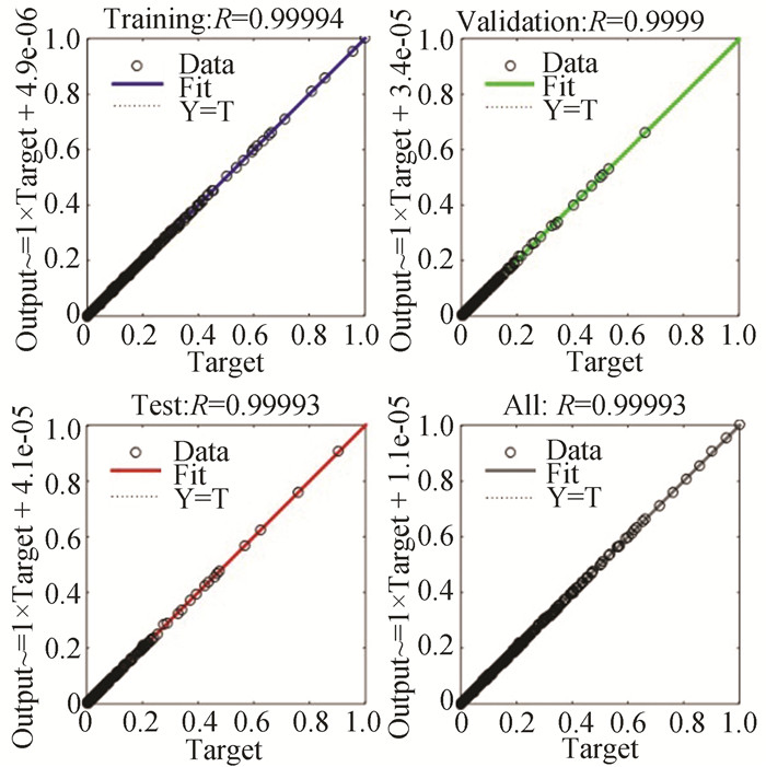
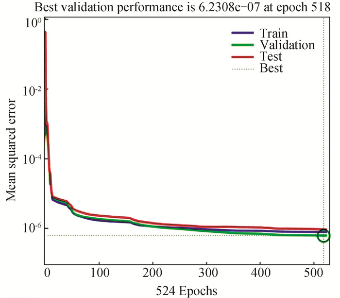
f) The accuracy and the performance of the proposed model is presented in Figs. 14-21 for 22 nm and 130 nm technology nodes and 300 K and 400 K temperature values respectively.
|
Fig.14 Performance plot of HSPICE simulations at 22 nm technology node (room temperature) |
|
Fig.15 Accuracy plot of HSPICE simulations at 22 nm technology node (room temperature) |

|
Fig.16 Performance plot of HSPICE simulations at 22 nm technology node (398.15 K) |

|
Fig.17 Accuracy plot of HSPICE simulations at 22 nm technology node (398.15 K) |
|
Fig.18 Performance plot of HSPICE simulations at 130 nm technology node (room temperature) |
|
Fig.19 Accuracy plot of HSPICE at 130 nm technology node (room temperature) |
|
Fig.20 Performance plot of HSPICE at 130 nm technology node (398.15 K) |
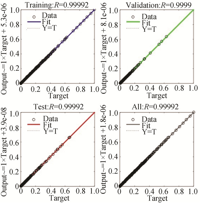
|
Fig.21 Accuracy plot of the HSPICE at 130 nm technology node (398.15 K) |
Following interpretations can be drawn from the above analysis done:
1) The proposed analytical model provides goodness of fit greater than 99% for technology nodes ranging from 22 nm-130 nm and temperatures ranging from 298.15 K-398.15 K.
2) Further, the results obtained from calculating MSE show that ANN simulation with analytical data is in excellent agreement with ANN simulation with HSPICE data, with error less than 1%.
3) Table 3 shows the improvement in the speed obtained utilising the proposed model for different temperatures at supply voltage of 1 V. The obtained results show that as the number of data points is increased, HSPICE simulation becomes slower (because of the number of parameters involved in simulation).
4) Moreover, it can be seen from Table 3 that speed improvement up to 80% is obtained when 5000 data points are considered.
6 ConclusionsArtificial Neural Networks were utilized in this paper to investigate their utility for designing circuits at ultradeep submicron technology node. The ANN was created to evaluate its capacity for mapping complicated functions and resolving challenges associated with rising non-linearity in the field of design. The neural network was constructed to map the design parameters to the delay parameters of a CMOS inverter. Datasets were produced using both equations and SPICE to determine how effectively the network responds to increasing levels of complexity. The ANN performed exceedingly well in all experiments, with a performance on test data close to 99.9%. This is a promising breakthrough in the field of circuit design since it demonstrates that an ANN can be effectively integrated with evolutionary algorithms such as PSO and ABC algorithms to tweak design parameters to attain the desired performance characteristics for various types of circuits.
| [1] |
Ratnesh R K, Goel A, Kaushik G, et al. Advancement and challenges in MOSFET scaling. Materials Science in Semiconductor Processing, 2021, 134: 106002. DOI:10.1016/j.mssp.2021.106002 (  0) 0) |
| [2] |
Mocuta A, Weckx P, Demuynck S, et al. Enabling CMOS scaling towards 3nm and beyond. In 2018 IEEE Symposium on VLSI Technology. Piscataway: IEEE, 2018, 147-148. DOI:10.1109/VLSIT.2018.8510683 (  0) 0) |
| [3] |
Radamson Henry H, Zhu Huilong, Wu Zhenhua, et al. State of the art and future perspectives in advanced CMOS technology. Nanomaterials, 2020, 10(8): 1555. DOI:10.3390/nano10081555 (  0) 0) |
| [4] |
Govindaraj V, Arunadevi B. Machine learning based power estimation for CMOS VLSI circuits. Applied Artificial Intelligence, 2021, 35(13): 1043-1055. DOI:10.1080/08839514.2021.1966885 (  0) 0) |
| [5] |
Maji K B, De B P, Kar R, et al. CMOS analog amplifier circuits design using seeker optimization algorithm. IETE Journal of Research, 2022, 68(2): 1376-1385. DOI:10.1080/03772063.2019.1649207 (  0) 0) |
| [6] |
Rout P K. Fast and Robust Design of CMOS VCO for Optimal Performance. Rourkela: National Institute of Technology, 2015.
(  0) 0) |
| [7] |
Behzad Moradi, Abdolreza Mirzaei. A new automated design method based on machine learning for CMOS analog circuits. International Journal of Electronics, 2016, 103(11): 1868-1881. DOI:10.1080/00207217.2016.1138538 (  0) 0) |
| [8] |
Delican Y, Vural R A, Yildirim T. Artificial bee colony optimization based CMOS inverter design considering propagation delays. In 2010 XIth international workshop on symbolic and numerical methods, modeling and applications to circuit design (SM2ACD). Piscataway: IEEE, 2010, 1-5. DOI:10.1109/SM2ACD.2010.5672326 (  0) 0) |
| [9] |
Mukhopadhyay Joyjit, Pandit Soumya. Modeling and design of a nano scale CMOS inverter for symmetric switching characteristics. VLSI Design, 2012, 2012(9): 9. DOI:10.1155/2012/505983 (  0) 0) |
| [10] |
Djeffal F, Chahdi M, Benhaya A, et al. An approach based on neural computation to simulate the nanoscale CMOS circuits: Application to the simulation of CMOS inverter. Solid-State Electronics, 2001, 51(1): 48-56. DOI:10.1016/j.sse.2006.12.004 (  0) 0) |
| [11] |
Huang Tianfu, Shi Xinchun, Sun Yuwei, et al. Three-phase photovoltaic grid-connected inverter based on feedforward decoupling control. Proceedings of the 2013 International Conference on Materials for Renewable Energy and Environment. Piscataway: IEEE, 2013, 2: 476-480. DOI:10.1109/ICMREE.2013.6893714 (  0) 0) |
| [12] |
Kumar P M, Sumanth Y, Ganesh S N V. Improving the power quality by MLCI type DSTATCOM. International Journal of Computer Applications, 2010, 10(1): 36-40. DOI:10.5120/1443-1952 (  0) 0) |
| [13] |
Ayers John E. Digital Integrated Circuits: Analysis and Design. Boca Raton: CRC Press, 2018.
(  0) 0) |
| [14] |
Mohammadi Ali, Mohammadi Mohammad, Zahiri Seyed Hamid. Design of optimal CMOS ring oscillator using an intelligent optimization tool. Soft Computing, 2018, 22(24): 8151-8166. DOI:10.1007/s00500-017-2759-4 (  0) 0) |
| [15] |
Kalra Shruti. On the mathematical insight of moderate inversion for ultradeep submicron CMOS technologies. Journal of Computational Electronics, 2018, 17(1): 205-210. DOI:10.1007/s10825-017-1109-1 (  0) 0) |
| [16] |
Nanoscale Integration and Modeling (NIMO) Group. Predictive technology model. http://ptm.asu.edu/.
(  0) 0) |
| [17] |
Mehdi Khosrow-Pour D B A. Advanced Methodologies and Technologies in Artificial Intelligence, Computer Simulation, and Human-Computer Interaction. Hershey: IGI Global, 2018. DOI:10.4018/978-1-5225-7368-5
(  0) 0) |
| [18] |
Bisi Manjubala, Goyal Neeraj Kumar. Artificial Neural Network Applications for Software Reliability Prediction. Hoboken: John Wiley & Sons, 2017.
(  0) 0) |
| [19] |
Chakraverty, Snehashish, Mall Susmita. Artificial Neural Networks for Engineers and Scientists: Solving Ordinary Differential Equations. Boca Raton: CRC Press, 2017.
(  0) 0) |
| [20] |
Dib Nihad. Umar Alsammarraie. Optimal design of symmetric switching CMOS inverter using symbiotic organisms search algorithm. International Journal of Electrical and Computer Engineering, 2020, 10(1): 171. DOI:10.11591/ijece.v10i1.pp171-179 (  0) 0) |
| [21] |
Liu W, Jin X, Chen J, et al. BSIM3v3.2.2 MOSFET Model User's Manual. Berkeley: University of California, Berkeley, 2005.
(  0) 0) |
| [22] |
Ichino Shinya, Teramoto Akinobu, Kuroda Rihito, et al. Statistical analysis of threshold voltage variation using MOSFETS with asymmetric source and drain. IEEE Electron Device Letters, 2018, 39(12): 1836-1839. DOI:10.1109/LED.2018.2874012 (  0) 0) |
| [23] |
Jan, Chia-Hong. Moore's law-Predict the unpredictable. Proceedings of the 2018 International Symposium on VLSI Technology, Systems and Application (VLSI-TSA). Piscataway: IEEE, 2018, 1-1. (  0) 0) |
| [24] |
Deepthi Amuru, Zahra Andleeb, Abbas Zia. Statistical variation aware leakage and total power estimation of 16 nm VLSI digital circuits based on regression models. International Symposium on VLSI Design and Test. Singapore: Springer, 2019: 565-578.
(  0) 0) |
| [25] |
Burden Frank, Winkler Dave. Bayesian regularization of neural networks. Artificial Neural Networks, 2008, 458: 23-42. (  0) 0) |
| [26] |
Suykens J A K, Vandewalle J. Least squares support vector machine classifiers. Neural Processing Letters, 1999(3): 293-300. (  0) 0) |
| [27] |
Thi Le Le, Nguyen Hoang, Dou Jie, et al. A comparative study of PSO-ANN, GA-ANN, ICA-ANN, and ABC-ANN in estimating the heating load of buildings' energy efficiency for smart city planning. Applied Sciences, 2019, 9(13): 2630. DOI:10.3390/app9132630 (  0) 0) |
| [28] |
Ahmadi Mohammadali, Chen Zhangxin. Machine learning-based models for predicting permeability impairment due to scale deposition. Journal of Petroleum Exploration and Production Technology, 2020, 10(7): 2873-2884. DOI:10.1007/s13202-020-00941-1 (  0) 0) |
 2023, Vol. 30


