2. The Institute of Microelectronics, Tsinghua University, Beijing 100084, China
The rapid development of many applications, such as big data, cloud computing and internet of things (IoT), leads to bandwidth exponential growth demand on data communication in both telecommunication system (backbone network) and local electronic system (chip-to-chip, backplane-to-backplane and multiple services)[1]. This increasing bandwidth demand has pushed serial-link towards data-rates of 40 Gb/s or beyond[2-6].
When data rate reaches 40 Gb/s, there are two main challenges encountering for design. One challenge is the timing budget extremely tight due to the ever decreased unit interval period. In the transmitter, the final stage serializer suffers from strict setup and hold time constraints at this high speed, so calibration loop[5, 7-9], and quarter-rate structures[10-11] are employed. To satisfy the jitter tolerance requirement while maintaining excellent jitter performance, a phase interpolator (PI) based digital clock and data recovery CDR are widely used due to its robustness, portability, and compactness[12-15]. In addition, the low jitter PLL is also required in system to provide high performance clock for both TX and RX. Another challenge is the channel loss including the parasitic of the bonding and electronic static discharge (ESD), dielectric loss and skin effect in cable and PCB trace, which all lead to inter-symbol interference (ISI). So the appropriate equalization scheme should be employed to compensate channel loss. Beside the two challenges mentioned above, the power and area efficient are still consideration for implementation.
This paper is focus on 40 Gb/s full SerDes transceiver with controller and PHY for very short range communication in data centre.
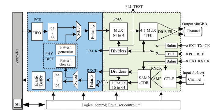
2 System ArchitectureFig. 1 shows the block diagram of the 40 Gb/s SerDes system architecture with controller, PCS and PMA. Transmitter in PMA contains low-speed 64:4 MUXs, high speed 4:1 MUXs, feed-forward equalization (FFE) and output driver. Receiver in PMA includes continuous-time linear equalizer (CTLE), PI based CDR and 16:64 DEMUXs. In order to improve power efficiency and relax timing budget, both TX and RX adopt quarter rate architecture. In addition, an LC-VCO based sub-harmonic injection locked PLL (SILPLL) with mixer-based injection timing control is used to provide a low jitter clock source for TX and RX[15].
|
Fig.1 Block diagram of the 40 Gb/s SerDes system architecture |
Both PCS and controller are synthesized by digital logic. The former mainly consists of PHY BIST (pattern generator and pattern checker), FIFO/Elastic buffer, 64/66 encoder and decoder, and polarity reversal circuit. The PHY BIST can generate and check the PRBS-7 pattern data. Besides that, the PCS supports P/N reverse to be convenience for practice application. The controller contains protocol transmission, forward error correction (FEC) and user layer BIST.
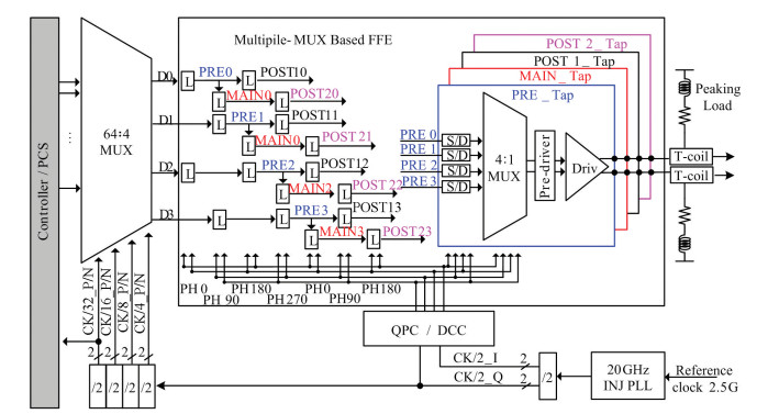
3 TransmitterA block diagram of the transmitter circuit is shown in Fig. 2. It consists of low-speed 64:4 MUXs, 4-tap multiple-MUX based FFE including latch arrays and a proposed 4:1 MUX, quadrature phase calibration (QPC) / duty cycle correction (DCC) circuits and a SILPLL with clock distribution. The 64 bit parallel data coming from the PCS are first multiplexed to yield four 10 Gb/s data streams in the low-speed 64:4 MUX circuit. The latch arrays use the quarter clocks to retime the input data and delay them with the proper UI space (the latch positions represent the signal's delay time) and finally generate 16-path quarter-rate data. The 16-path data are feed into the following four 4:1 MUXs to generate four full-rate data streams, which are delayed one UI space at full rate speed. After firstly buffered by pre-drivers, the four data streams are sent to the 4-tap FFE for equalization. In addition to, the QPC and DCC of the quadrature clocks are needed due to the 4:1 MUX being sensitive to quadrature phase mismatch and duty cycle distortion[2].
|
Fig.2 Block diagram of the transmitter |
The main feature of the transmitter is utilizing 4-tap multi-MUX based FFE, which not only extremely relaxes the stringent timing requirement of the final serialization stage, but also saves the power due to halving the maximum clock speed and replacing the final two-stage 2:1 multiplexers (MUXs) and the retiming latches with one 4:1 MUX. Furthermore, a novel low power 4:1 MUX is proposed to further improve the jitter performance. The details of the proposed 4:1 MUX are present below.
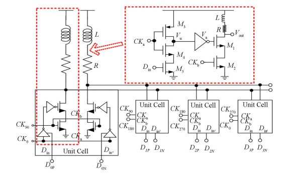
Fig. 3 depicts a block diagram of the proposed 4:1 MUX. It consists of peaking-loads and four unit cells, which are activated sequentially by four quadrature clocks. Each unit cell contains a differential pair of pulse generator. The detail of the pulse generator is illustrated in Fig. 3 dash box. The pulse generator contains two cascade sampling stages. The first sampling stage consisting of three stack transistors is as a latch, while the second sampling stage consisting of two transistors is as the output stage. Here, CKa and CKb are quadrature clock and CKa is ahead CKb 90 degree phase. Din is the quarter-rate input data and Vout is the pulse generator output. The logic function of the pulse generator is as follows:
| $ {V_{{\rm{ out }}}} = \overline {C{K_{\rm{a}}} \cdot C{K_{\rm{b}}} \cdot {D_{{\rm{ in }}}}} = \overline {C{K_{\rm{a}}}} + \overline {C{K_{\rm{b}}}} + \overline {{D_{{\rm{in}}}}} $ | (1) |
|
Fig.3 The proposed 4:1 MUX with the pulse generator details |
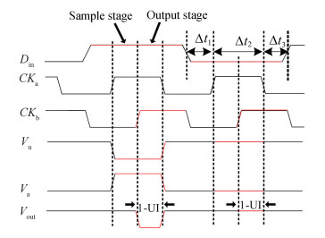
It is noted that when just analyzing the circuit details of the pulse generator, the intermediate node Vu is considered as an uncertain state at the time of Din is low and CKa is high. However, the 4:1 MUX is a sequential circuit. When feeding the data into the 4:1MUX, the data are firstly retimed and delayed with proper time by latch arrays. In order to guarantee the proper serialization, the data transitions only occur at the negative pulse of the CKa (see Fig. 4). In addition, the timing constraint can effectively avoid the uncertain state occurring at the intermediate node (Vu).
|
Fig.4 Timing diagram of the proposed pulse generator in 4:1 MUX |
Fig. 4 also gives the timing diagram of the uncertain state under the timing constraint. In the first stage Δt1, the intermediate node Vu is a certain state and its value is high. When the rising edge of the CKa arrives, Vu entrances the uncertain state. However, Vu still keeps high during the positive of CKa (in the second stage Δt2). Because the electric charge leakage of the MOS (reducing Vu's electric charge) is very little in this technology and the clock feed-through of CKa (increasing Vu's electric charge) cannot exceed the threshold value. When the falling edge of the CKa arrives, Vu returns into the certain state and its value is high in the stage of Δt3. Therefore, the uncertain state can be effectively avoided in the timing constraint.
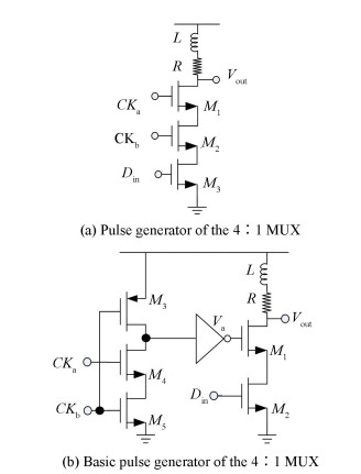
Fig. 5(a) gives another pulse generator of the 4:1 MUX[16]. The pulse generator adopts three stacked transistors to generate a narrow output pulse. Comparing with the proposed pulse generator, although it can save power, it has to be large enough size to provide the needed current drive, which inevitable increases the output capacitance and reduces its bandwidth. Fig. 5(b) gives another basic pulse generator of the 4:1 MUX[17]. It separates the ANDing and sampling operations into two stages. Although the output capacitance is reduced, the intermediate inverter needs a 25% duty-cycle pulse every clock period to driver the output stage. In order to have enough bandwidth, the output of the inverter needs sharp enough edges, which needs large size transistor and is power hunger. However, the proposed 4:1 MUX not only reduces the output stage, but also improves the power efficiency due to only using 50% duty clock.
|
Fig.5 Schematic of other pulse generators |
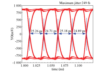
Fig. 6 shows the simulation results of the proposed 4:1 MUX using the calibrated clocks. The four horizontal eye widths of the 4:1 MUX are almost identical, and its maximum jitter is 249 fs. The simulation results of the proposed 4:1 MUX show that it has better jitter performance than that of the 4:1 MUX in Ref.[17].
|
Fig.6 Eye diagram of the 4:1 MUX output after buffer |
4 Receiver
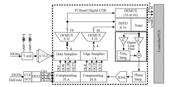
Fig. 7 shows a block diagram of the RX circuit, which mainly consists of T-coil, 2-stage CTLE, PI based digital CDR, and clock input circuit. The T-coil is used to extent the bandwidth of the analog front-end. The input data passing the T-coil is firstly equalized by the CTLE and then feeds them into the CDR. The CDR utilizes the eight-phase clocks to sample the input data information and then uses 16 BBPDs and a majority voter to extract the phase error between the input data and the local clock. After being filtered and accumulated by the digital loop filter and phase integration, the EARLY/LATE information rotates the PI by 6 bit current digital-to-analog converter (DAC) for tracking the input data phase. Finally, these recovered 16 path data are deserialized and then are sent to the PCS. At the same time, the recovered clock is divided to 625 MHz and also is sent to PCS.
|
Fig.7 Block diagram of the receiver |
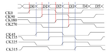
The main features of the CDR are utilizing the quarter-rate architecture to relax the tight timing of the sampling front-end, and employing both the 2nd order digital filter and compensating PI to improve the CDR performance. Fig. 8 shows the timing diagram of the quadrature sampling. By adopting the 2nd order loop, the CDR not only enlarges the jitter tolerance but also reduces the self-generated hunting jitter. Besides that, to further reduce the self-generated hunting jitter, this design uses compensating PI to improve the linearity between the input phase code and output clock's rotated phase. This is because the nonlinearity of the PI introduces a much larger phase jump in differential path and makes the data-sampling clock drifting away from the optimal decision points. The details of the CDR with the compensating PI design can get from Ref.[18].
|
Fig.8 Timing diagram of the quadrature sampling |
5 Measurement Results
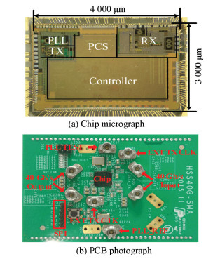
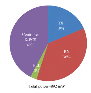
The full transceiver with controller and PHY is implemented in a 65 nm CMOS technology and adopts chip on board (COB) package. The controller and PCS are synthesized by digital logic. Fig. 9(a) shows the micrograph of the full chip and the test PCB is illustrated in Fig. 9(b). The full chip occupies an area of 3 mm×4 mm, where the core area of the TX including PLL and the RX are 1.01 mm×1.12 mm and 1.92 mm×1.2 mm respectively. The controller and PCS together consume 375 mW from 1.0 V supply and the PMA consumes 517 mW from 1.2 V supply at 40 Gb/s. Power breakdown of the full transceiver is shown in Fig. 10.
|
Fig.9 Micrograph of the full chip and the test PCB |
|
Fig.10 Full chip power breakdown |
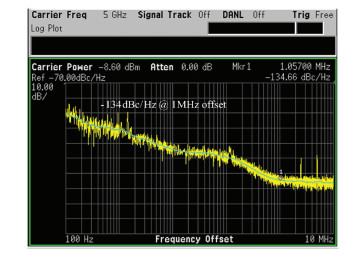
The phase noise of the 20 G SILPLL with quarter-rate output at 5 GHz is measured with Agilent E4440A and shown in Fig. 11. Its phase noise is -134dBc/Hz at 1 MHz frequency offset. In addition to, the SILPLL can lock from 18.6 GHz to 22.7 GHz with 3 bit switch-capacitor.
|
Fig.11 Measured SILPLL phase noise with quarter-rate output at 5 GHz |
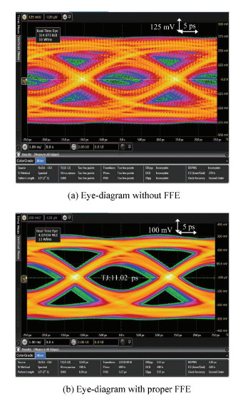
The transmitter output is measured with Agilent DSA-X 93204A (32 GHz bandwidth) after a channel consisting of a 900 μm double bonding wire, a 3.2 cm PCB trace, a 2.92 mm connector with 40 GHz bandwidth and a 0.5 m cable. Measurement result shows that this channel has 9.7 dB insert loss. Fig. 12(a) and (b) give the eye-diagrams of the PHY BIST transmitting 40 Gb/s PRBS-7 pattern before and after applying the 4-tap FFE obviously, and the FFE can significantly improve the eye quality. After using the optimal equalization coefficients (Pre=421 mV, Main=642 mV, Post1=494 mV and Post2=387 mV), the eye width and eye height are optimized to 0.55UI and 192 mV, respectively. The total jitter is 11.2 ps.
|
Fig.12 PHY_BIST transmitting 40 Gb/s PRBS7 over -9.7dB channel loss |
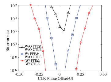
The receiver measurement setup is that, the TX transmits 40 Gb/s PRBS-7 with pattern generator in PHY BIST and the RX receives it and checks with pattern checker after a complex channel, which has 15.3 dB insert loss. This channel contains two double bonding wires, two connectors, 6.3 CM PCB trace and a 0.5 m connecting cable. The receiver BER bathtub curves are measured with different equalization schemes after turning off the CDR. As indicated in Fig. 13, at first the FFE and CTLE are both disabled, the measured BER is above 1e-6; then only the FFE is active with the optimal equalization coefficients, which are got from the TX eye-diagram measurement, the eye opening reaches 0.18UI for BER=1e-12. At last, both the FFE and CTLE are active with optimal equalization coefficients (Voltage of the CTLE is 860 mV), the eye opening can reach 0.41 UI for BER=1e-12. When using the user layer BIST, the BER can lower 1e-14 and the efficient bandwidth is above 38.1 Gb/s, this is because of the protocol frame head and tail, FEC and 64/66 encoder consuming part bandwidth.
|
Fig.13 Measured receiver BER bathtub curve |
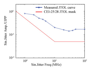
The RX performance is also demonstrated by the jitter tolerance test at 28 Gb/s as shown in Fig. 14, along with the CEI-25G/28G JTOL mask[19]. The measurement setup is that, the RX uses the external clock to receive the PRBS-7 data pattern generated by Tektronix BSA286C and uses the PHY BIST to checks the BER. Measured at the BER threshold of 2.5e-9, the out-of-band jitter tolerance at 100 MHz is 0.17 UI.
|
Fig.14 Measured receiver jitter tolerance curve at 28 Gb/s |
Table 1 describes the performance comparison of transceiver. Relative to the other design, the present transceiver features a much better jitter performance and power efficiency.
| Table 1 Performance summary |
6 Conclusions
This paper implements a 40 Gb/s SerDes transceiver chip with controller and PHY. The TX adopts multiple-MUXs based 4-tap FFE with a proposed 4:1 MUX, and the RX employs a PI based CDR with BBPD. The measurement results show that the transceiver can achieve BER < 10-12 at 40 Gb/s over a 15.3 dB channel loss.
| [1] |
Singh U, Garg A, Raghavan B, et al. A 780 mW 4×28 Gb/s transceiver for 100 GbE gearbox PHY in 40 nm CMOS. IEEE Journal of Solid-State Circuits, 2014, 49(12): 3116-3129. DOI:10.1109/JSSC.2014.2352299 (  0) 0) |
| [2] |
Chen M S, Yang C K K. A 50-64 Gb/s serializing transmitter with a 4-tap, LC-ladder-filter-based FFE in 65 nm CMOS technology. IEEE Journal of Solid-State Circuits, 2015, 50(8): 1903-1916. DOI:10.1109/JSSC.2015.2411625 (  0) 0) |
| [3] |
Chiang P C, Jiang J Y, Hung H W, et al. 4x25 Gb/s transceiver with optical front-end for 100 GbE system in 65 nm CMOS technology. IEEE Journal of Solid-State Circuits, 2015, 50(2): 573-585. DOI:10.1109/JSSC.2014.2365700 (  0) 0) |
| [4] |
Lee J, Chiang P C, Peng P J, et al. Design of 56 Gb/s NRZ and PAM4 SerDes transceivers in CMOS technologies. IEEE Journal of Solid-State Circuits, 2015, 50(9): 2061-2073. DOI:10.1109/JSSC.2015.2433269 (  0) 0) |
| [5] |
Chian P C, Hung H W, Chu H Y, et al. 2.3 60Gb/s NRZ and PAM4 transmitters for 400GbE in 65nm CMOS. Proceedings of the 2014 IEEE International Solid-State Circuits Conference Digest of Technical Papers (ISSCC). Piscataway: IEEE, 2014.42-43. DOI: 10.1109/ISSCC.2014.6757329.
(  0) 0) |
| [6] |
Chen M S, Shih Y N, Lin C L, et al. A fully-integrated 40-Gb/s transceiver in 65-nm CMOS technology. IEEE Journal of Solid-State Circuits, 2012, 47(3): 627-640. DOI:10.1109/JSSC.2011.2176635 (  0) 0) |
| [7] |
Kanda K, Tamura H, Yamamoto T, et al. A single-40 Gb/s dual-20 Gb/s serializer IC with SFI-5.2 interface in 65 nm CMOS. IEEE Journal of Solid-State Circuits, 2009, 44(12): 3580-3589. DOI:10.1109/JSSC.2009.2031030 (  0) 0) |
| [8] |
Kaeriyama S, Amamiya Y, Noguchi H, et al. A 40 Gb/s multi-data-rate CMOS transmitter and receiver chipset with SFI-5 interface for optical transmission systems. IEEE Journal of Solid-State Circuits, 2009, 44(12): 3568-3579. DOI:10.1109/JSSC.2009.2031026 (  0) 0) |
| [9] |
Huang K, Wang Z Q, Zheng X Q, et al. A 75 mW 50 Gbps SerDes transmitter with automatic serializing time window search in 65 nm CMOS technology. Proceedings of the IEEE International Conference on Custom Integrated Circuits Conference. Piscataway: IEEE, 2014. DOI: 10.1109/CICC.2014.6946101.
(  0) 0) |
| [10] |
Kim J, Balankutty A, Elshazly A, et al. A 16-to-40Gb/s quarter-rate NRZ/PAM4 dual-mode transmitter in 14nm CMOS. Proceedings of the IEEE International Conference on Solid-State Circuits Conference. Piscataway: IEEE, 2015. 61-62.DOI: 10.1109/ISSCC.2015.7062925.
(  0) 0) |
| [11] |
Hafez A A, Cheng M S, Ken Yang C K. A 32-to-48 Gb/s serializing transmitter using multiphase serialization in 65 nm CMOS. Proceedings of the 2013 IEEE International Solid-State Circuits Conference Digest of Technical Papers (ISSCC). Piscataway: IEEE, 2013. 38-40.DOI: 10.1109/ISSCC.2013.6487627.
(  0) 0) |
| [12] |
Raghavan B, Cui D, Singh U. A sub-2 W 39.8-44.6 Gbps transmitter and receiver chipset with SFI-5.2 interface in 40 nm CMOS. IEEE Journal of Solid-State Circuits, 2013, 48(12): 3219-3228. DOI:10.1109/JSSC.2013.2279054 (  0) 0) |
| [13] |
Shu G H, Choi W S, Saxena S, et al. A 4-to-10.5Gb/s 2.2 mW/Gb/s Continuous-Rate Digital CDR with Automatic Frequency Acquisition in 65nm CMOS. Proceedings of the IEEE International Conference on Solid-State Circuits Conference Digest of Technical Papers. Piscataway: IEEE, 2014. 150-152.DOI: 10.1109/ISSCC.2014.6757377.
(  0) 0) |
| [14] |
Gangasani G R, Hsu C M, Bulzacchelli J F. A 16-Gb/s backplane transceiver with 12-tap current integrating DFE and dynamic adaptation of voltage offset and timing drifts in 45-nm SOI CMOS technology. IEEE Journal of Solid-State Circuits, 2012, 47(8): 1828-1841. DOI:10.1109/JSSC.2012.2196313 (  0) 0) |
| [15] |
Zheng X Q, Zhang C, Lv F X, et al. A 40-Gb/s quarter-rate SerDes transmitter and receiver chipset in 65-nm CMOS. IEEE Journal of Solid-State Circuits, 2017, 52(11): 2963-2978. DOI:10.1109/JSSC.2017.2746672 (  0) 0) |
| [16] |
Chiang P, Dally W J, Lee M J E, et al. A 20-Gb/s 0.13-m CMOS serial link transmitter using an LC-PLL to directly drive the output multiplexer. IEEE Journal of Solid-State Circuits, 2005, 40(4): 1004-1011. DOI:10.1109/JSSC.2004.842841 (  0) 0) |
| [17] |
Zheng X Q, Zhang C, Lv F X, et al. A 5-50 Gb/s quarter rate transmitter with a 4-tap multiple-MUX based FFE in 65 nm CMOS. Proceedings of the IEEE International Conference on Asian Solid-State Circuits Conference.Piscataway: IEEE, 2016.305-308. DOI: 10.1109/ESSCIRC.2016.7598303.
(  0) 0) |
| [18] |
Zheng X Q, Zhang C, Yuan S, et al. An improved 40 Gb/s CDR with jitter-suppression filters and phase-compensating interpolators. Proceedings of the IEEE International Conference on Asian Solid-State Circuits Conference. Piscataway: IEEE, 2016. 85-88. DOI: 10.1109/ASSCC.2016.7844141.
(  0) 0) |
| [19] |
Optical Internetworking Forum. IA title: Common electrical I/O (CEI)—Electrical and jitter interoperability agreements for 6G + bps, 11G + bps and 25G + bps I/O. http://www.oiforum.com/public/documents/OIF_CEI_03.1.pdf.
(  0) 0) |
| [20] |
Navid R, Chen E H, Hossain M, et al. A 40 Gb/s serial link transceiver in 28 nm CMOS technology. IEEE Journal of Solid-State Circuits, 2015, 50(4): 814-827. DOI:10.1109/JSSC.2014.2374176 (  0) 0) |
 2019, Vol. 26


