2. National Key Laboratory of Science and Technology on Advanced Composite in Special Environments, Harbin Institute of Technology, Harbin 150001, China;
3. Center of Analysis and Measurement, Harbin Institute of Technology, Harbin 150001, China
Transparent conducting oxides (TCOs) are widely used in solar cells, displays, gas-sensitive components, antistatic coatings, and semiconductors because of their similar conductivity with metal, high transmittance in the visible light range, high infrared reflectance, and semiconductor characteristics[1-5]. They have gradually become indispensable functional device in various electronic products in the information age. Among various TCO thin film materials, tin-doped indium oxide (In2O3∶Sn) thin film is the material with the best comprehensive performance and the widest application range. The indium-tin-oxide (ITO) film grown by the conventional deposition method is a heavily doped, highly degenerated n-type semiconductor transparent conductive oxide film material. It has multiple unique optical characteristics, such that its forbidden band width is greater than 3.5 eV, resistivity is as low as 10-4 Ω ·cm, ultraviolet cutoff (ultraviolet absorption rate) is greater than 85%, high visible light transmittance is more than 85% at 550 nm wavelength, and high infrared reflection rate is greater than 80%[6-7]. Therefore, it is widely used in many industries such as flat panel displays, light emitting diodes, thin film transistors, thermal mirrors, and electrochromic devices[8-10]. However, untreated In2O3∶Sn film has a lower work function which can result in a high energy barrier that hinders the passage of carriers through the interface[11], thus leading to poor overall performance of directly prepared devices. Therefore, it has become more and more important to improve the Fermi level of In2O3∶Sn film by interface engineering method.
In order to solve the problem of low work function of TCO film, researchers have developed a variety of interface engineering methods, which can improve the work function of ITO and reduce the hole injection barrier, thereby reducing the driving voltage and increasing the hole injection efficiency, consequently improving the overall efficiency of device. Harvey et al.[12] studied the modification of surface dipoles on TCOs with bixbyite structure, and the work function can be increased by a high temperature oxygen exposure. Helander et al.[13] prepared the surface-functionalized ITO and demonstrated a chlorinated ITO transparent electrode with a work function larger than 6.1 eV. Lin et al.[14] investigated the effects of a KrF excimer laser irradiation on the surface work function (SWF) of ITO. Among these methods, oxygen plasma treatment is the most effective in improving the work function of In2O3∶Sn thin films, but the high temperature preparation conditions will reduce the performance of the substrate, and the oxidation conditions will cause film aging effect, which deteriorates device performance. Meanwhile, the understanding of the change mechanism of work function after surface oxidation treatment is not uniform[15-16]. In addition, the work function shows obvious timeliness after oxygen plasma treatment, that is, the work function quickly decreases or even returns to the initial value as the storage time increases. The cause and the physical mechanism of this problem are not clear. Hence, it is urgent to find a new method with no aging effect to enhance work function with enough experimental data and further analyze the work function mechanism.
In this study, conventional magnetron sputtering with new-type Ar+ plasma exposure technique was applied to deposit the preferentially oriented In2O3∶ Sn thin films in order to improve the work function and solve the double technical problems of high temperature and aging effect when fabricating In2O3∶Sn films. The X-ray diffraction (XRD), ultraviolet photoemission spectroscopy (UPS), and X-ray photoelectron spectroscopy (XPS) measurements were adopted to clarify the mechanism of the change in the work function of In2O3∶Sn thin film by changing the deposition conditions of the Ar+ plasma bombardment.
1 Experiment 1.1 Film PreparationThe materials in the experiment include: high purity In2O3∶Sn target (Sn atom content 10 at.%, purity 99.99%, φ 49 mm×3 mm), argon gas (purity 99.99%), high resistance glass, P type (100) silicon wafer (thickness 740 μ m, size 10 mm×10 mm), polished hot pressed zinc sulfide (14 finish, φ 20 mm×8 mm), deionized water, absolute alcohol (purity 99.7%), and acetone (purity 99.7%).
Preparation: The magnetron sputtering deposition system was designed using an RF power supply (13.56 MHz) with a negative bias voltage between -400 V and -900 V. Under a unipolar pulsed DC power supply, a 50% duty cycle was applied to the substrate at a frequency of 50 kHz. A 2-inch diameter hot-pressed In2O3∶Sn target was deposited by magnetron sputtering on a borosilicate glass. Typical sputtering conditions are as follows: base pressure was less than 2×10⁻⁴ Pa, target-substrate distance was 70 mm, argon pressure was 0.5 Pa, and argon flow rate was 100 standard cubic centimeters per minute (SCCM). The target was pre-sputtered for 20 min and then deposited at the same power level as the 20 W sputtering power. The entire process of deposition was set as 25 min at room temperature.
Another deposition method is plasma bombardment assisted magnetron sputtering. The deposition process consists of two steps: a sputtering step and a plasma bombardment step, where one sputtering step plus one plasma bombardment step constitutes one cycle. The parameters of the sputtering step were kept constant, and the power was kept at 20 W. Subsequently, the RF power was closed and a metal baffle was placed between the In2O3∶Sn and the substrate to prevent the target from being affected during plasma bombardment. The plasma bombardment step was provided by a single-stage pulsed DC power supply with a negative bias (|Vp|) varying between |-400 V|~|-900 V| at a current frequency of 50 kHz, and the duty cycle (continuous Time) was kept at 50%. The ratio of the plasma bombardment step to the magnetron sputtering deposition step time was maintained at 2, and the entire period of time was 75 min, which includes a total of 5 cycles.
1.2 CharacterizationThe thickness of the film was measured using Talysurf PGI 1240 profilometer with a resolution of 0.8 nm. The crystal structure of the film was measured by using scanning incident X-ray diffraction (GIXRD, PANalytical X'Pert Pro) equipped with an X-ray source for a Cu target that produces K α rays at a wavelength of 1.54 Å. The voltage and current were 40 kV and 20 mA respectively, and the step angle for scanning was 0.05°.
The surface energy states of the chemical bonding states or work functions of the In2O3∶Sn film were subjected to low-energy X-ray measurement under ultra-high vacuum conditions using a Thermo ESCALAB 250 X-ray photoelectron spectrometer. Taking a single-color Al K α target as a low-energy X-ray source, the energy (hυ) produced was 1486.6 eV. A He I (21.2 eV) with an energy resolution of about 0.1 eV was used as an excitation source to obtain a UPS for determining the work function.
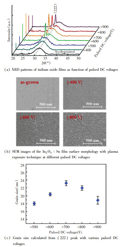
2 Results and Discussions 2.1 Crystal Structure of In2O3∶SnFig. 1(a) shows the crystal structure of the In2O3∶Sn films deposited by different plasma energy bombardment assisted magnetron sputtering. It can be found that the crystal structure of the In2O3∶Sn film was amorphous when the negative bias voltage was low (|Vp| < |-500 V|), which was not significantly different from the structure of the In2O3∶Sn film prepared by direct magnetron sputtering. When |-500 V| < |Vp| < |-700 V|, the positively charged argon ions were accelerated by the negative bias to impact the surface of the film, and the kinetic energy was converted into the energy of partial internal energy and surface atomic motion. Therefore, the surface atom mobility was increased, and the surface of the In2O3∶Sn crystallized to reveal the (222) crystal plane. The Sn atoms in the film entered the doping position, resulting in no obvious SnO2 peak. When |Vp| > |-700 V|, no crystal orientation transition occurred under argon ion bombardment, while (222) peak intensity decreased. It indicates that the energy that caused the crystal orientation transition was increased due to the doping action. When |Vp|=|-900 V|, it was difficult for the energy provided by Ar+ to meet its preferred orientation transition requirements, but it caused damage to the < 222 > crystal orientation.
|
Fig.1 Crystal structure of In2O3∶Sn thin film |
Fig. 1(b)-(c) shows the grain size change of the In2O3∶Sn film prepared by different plasma energy bombardment assisted magnetron sputtering. According to Fig. 1(b), with the increase of negative bias pressure, the surface particle size showed an increasing trend, whereas the particle size changed from dispersion distribution to agglomeration distribution. Under low negative bias, the main function of argon ion bombardment is to enhance the migration of surface atoms and eliminate surface defects, leading to uniform and dense surface characteristics. Under high argon ion bombardment energy, the main function is to irradiate the surface, resulting in "thousands of gullies" of island structure on the surface of In2O3∶Sn film. As shown in Fig. 1(c), as the negative bias increased, the grain size of the In2O3∶Sn film increased first. When |Vp|=|-700 V|, the grain size was up to ~23.1 nm. As the bias voltage continued to increase, the grain size gradually decreased. The results were consistent with the results of the XRD and SEM patterns.
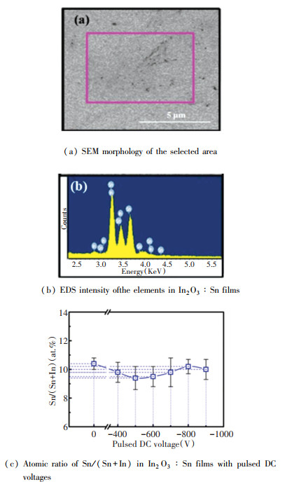
2.2 Compositional Characterization of In2O3∶Sn Thin FilmsThe proportional relationship of the contents of In, Sn, and O in the In2O3∶Sn film was adjusted by changing the magnitude of the negative bias. The ratio of Sn and In elements in the In2O3∶Sn film was calibrated using an X-ray energy spectrometer (EDS).
Fig. 2 shows the SEM surface topography of the selected area of the In2O3∶Sn film prepared on the glass surface with the negative bias voltage of |-600 V| and the typical In and Sn energy peaks in the EDS of the film surface. According to EDS analysis, the atomic ratio of Sn∶In deposited by plasma bombardment assisted deposition of In2O3∶Sn film did not occur with the change of negative bias (|-400 V| < |Vp| < |-900 V|), while great changes can be seen within the margin of error.
|
Fig.2 Compositional characterization of In2O3∶Sn films |
2.3 Chemical Bonding State of In2O3∶Sn Thin Films
Fig. 3 shows the core level spectrum of In2O3∶Sn film In 3d prepared with different negative biases (|-500 V| and |-800 V|). There are two peaks in the In2O3∶Sn film In 3d, the 3d5/2 peak at ~444.4 eV and the 3d3/2 peak at ~452.0 eV[17-18]. The presence of the doublet of the In element (3d3/2 and 3d5/2) can be observed in Fig. 3. It is the result of the splitting of indium orbital electrons after the spin process. For the two peaks, the peak of the low-angle quantum number after the general spin split had a higher binding energy, and that of the high-angle quantum number had a lower binding energy. Moreover, in the peak of the indium element, the peak intensity corresponding to the high-angle quantum number was also higher than that corresponding to the low-angle quantum number. Similar phenomena have been found in transition metal elements such as Cd and Y. As illustrated in Fig. 3, as the negative bias increased, a small amount of displacement (~0.3 eV) occurred at the peak position of In. It may be because the original unsaturated In-O bond is gradually combined during high-energy plasma bombardment, and the new free oxygen makes the bonding of the In-O bond stronger, so the bonding bond can shift toward the high energy direction. Meanwhile, it was found that the position between the 3d5/2 peak and the 3d3/2 peak remained basically the same, which was similar to the results in other literature.

|
(a) As-grown; (b) |-500 V|; (c) |-800 V| Fig.3 Deconvolutions of In 3d spectra in In2O3∶Sn films as function of pulsed DC voltages |
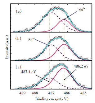
Subsequently, a high-resolution XPS analysis of the bond energy region of Sn 3d5/2 was performed. Fig. 4 shows the Sn 3d partial peak fit diagram of the In2O3∶Sn film prepared under |Vp|=|0 V|, |Vp|=|-500 V|, and |Vp|=|-800 V|, respectively. After the partial peak fitting, it can be concluded that the fitted graph contains two peaks, i.e. ~486.2 eV and ~487.1 eV, corresponding to two different oxidation states of Sn∶ Sn2+ (~486.2 eV) and Sn4+ (~487.1 eV)[19]. It was observed that the concentration of Sn4+ gradually increased with the increase of the negative bias, while the Sn2+ peak showed a significant downward trend. This is because as the negative bias increases, the energy of the bombardment of the sample surface by the Ar+ plasma gradually increases, so that the doped Sn2+ ions in the film further lose electrons to the Sn4+ high energy state under Ar+ bombardment. The transition of Sn2+ ions to Sn4+ ions can also be considered as an increase in the position of the Sn3+ ions in place of the In3+ ions, thus there are more freely mobile electrons in the entire film layer.
|
(a) As-grown; (b) |-500 V|; (c) |-800 V| Fig.4 Deconvolutions of Sn 3d5/2 spectra in In2O3∶Sn films as function of pulsed DC voltages |
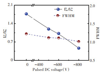
The ISn2+/ISn4+ ratio and the full width at half maximum of the Sn4+ peak of the In2O3∶Sn film prepared under different negative biases are shown in Fig. 5. It can be seen from the figure that with the increase of the negative bias, the ratio of ISn2+/ISn4+ gradually decreased from 1.75 to 0.3, and the half-height of the Sn4+ peak narrowed accordingly from ~1.2 to ~1.0. It can be proved that the plasma bombardment process contributes to the conversion of low-priced Sn2+ to high-priced Sn4+.
|
Fig.5 ISn2+/ISn4+ and FWHM of Sn4+ in In2O3∶Sn films as a function of Vp |
2.4 Work Function of In2O3∶Sn Thin Films
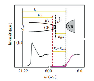
The basic band structure of the n-type In2O3∶Sn film prepared in the experiment is presented in Fig. 6. It can be found that the intrinsic band gap (Eg0) is expressed as the energy difference between the valence band top and the conduction band bottom (Eg0=ECBM-EVBM). When visible light was transparent, the minimum energy was ~3.1 eV. However, for most depolarizing semiconductors like In2O3∶Sn, due to the high degree of differentiation of the conduction band, (EF-EVBM) is broadened and its effective band gap is much larger than 3.1 eV. Among them, EF represents the Fermi level and EVBM represents the top of the price band. Changes in (EF-EVBM) can be well explained by the Burstein-Moss transition. In general, the larger the value of (EF-EVBM) is, the larger the carrier concentration is, and the better the conductivity of the In2O3∶Sn film is.
|
Fig.6 Schematics of typical In2O3∶Sn thin films band structure |
Work function (WF) refers to the energy difference from the Fermi level to the vacuum level (WF=Evac-EF). The value can also be expressed by the difference in ion potential energy (Ip=Evac-EVBM) minus (EF-EVBM). If the ion potential energy is a fixed value (Ip=Evac-EVBM=Constant), then the relationship between the work function of the film and (Evac-EVBM) is a linear function with a slope of -1, which is an intercept of Ip. Therefore, work function (WF) can be expressed as
| $ {W_{\rm{F}}} = - ({E_{\rm{F}}} - {E_{{\rm{VBM}}}}) + {I_p} $ | (1) |
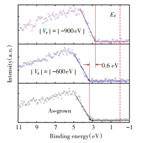
Fig. 7 shows the UPS spectra of the In2O3∶Sn film prepared under different negative biases. With the increase of the negative bias, although the content of oxygen vacancies in the In2O3∶Sn film was reduced, it did not reduce the carrier concentration in the In2O3∶Sn film. The reason is that the excellent electrical properties of the In2O3∶Sn film are not caused by the supply of excess free electrons mainly resulted from a large number of oxygen vacancies, but by the doped Sn atoms which lead to an increase in free electrons. After plasma bombardment, the low-energy Sn2+ in the In2O3∶Sn film would continue to lose the electrons into a high-energy Sn4+, which provides more free electrons for the film, and further improves the conductivity of the film. However, as the negative bias continued to rise (>|-700 V|), the bombardment of the film by high-energy Ar+ ions caused the surface of the film to be damaged by radiation, leading to an increase in defects in the film, a decrease in carrier concentration, and eventually a shift in the Fermi level to a low level.
|
(a)As-grown; (b)|Vp|=|-600 V|; (c)|Vp|=|-900 V| Fig.7 UPS spectra of In2O3∶Sn thin films prepared by plasma exposure technique under different pulsed DC voltages |
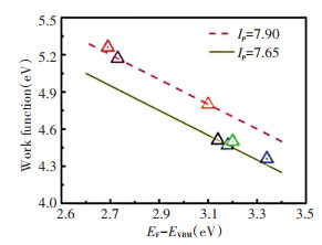
Fig. 8 depicts the relationship between the work function and (EF-EVBM) of In2O3∶Sn thin film prepared by plasma bombardment assisted magnetron sputtering under different negative bias voltages. Assuming that the effect of the surface dipole on the work function is eliminated, the ion potential energy should be a constant, and the data points of all work functions and (EF-EVBM) relationships should fall on the line WF=-(EF-EVBM)+Ip. The In2O3∶Sn film was in good agreement with the WF=-(EF-EVBM)+Ip relationship. First, as the negative bias voltage increased, the crystal structure of the film was improved, while the Sn2+ low energy state was converted to the high valence state of Sn4+, which increased the carrier concentration. Ip was maintained near 7.85 eV, and (EF-EVBM) increased from 3.14 eV to 3.34 eV, resulting in a decrease in work function. When |Vp|>|-700 V|, the decrease in carrier concentration was caused by the damage to the internal structure of the film, and the work function was improved. The maximum work function of 5.1 eV was generated at (EF-EVBM) equal to 2.69.
|
Fig.8 Relation between work function and Fermi level position (EF-EVBM) of In2O3∶Sn thin film using Ar+ plasma exposure with various pulsed DC voltages |
3 Conclusions
A high work function In2O3∶Sn film was prepared by plasma bombardment assisted magnetron sputtering to realize simple preparation of transparent conductive film at room temperature. The work function of the In2O3∶Sn film was significantly affected by the Ar+ plasma bombardment applied by DC pulse voltage. For the In2O3∶Sn film with |Vp|=|-500 V|, the enhanced adsorption atom mobility eliminated defects and improved the formation of surface crystallites. The increase of the work function of In2O3∶Sn thin film was because the oxidation state of the low-value Sn2+ gradually changed to the oxidation state of the high-valence Sn4+, which resulted in an increase in oxygen on the surface of In2O3∶Sn. Due to low temperature deposition and inert atmosphere, this study solved the problems of the degradation of film substrate performance and the aging effect of high temperature plasma deposition. In addition, it explained part of the mechanisms of In2O3∶Sn work function change using a variety of testing methods. These results provide technical reserve and theoretical basis for the application of In2O3∶Sn thin films in the field of semiconductors.
| [1] |
Liu H Y, Avrutin V, Izyumskaya N, et al. Transparent conducting oxides for electrode applications in light emitting and absorbing devices. Superlattices and Microstructures, 2010, 48(5): 458-484. DOI:10.1016/j.spmi.2010.08.011 (  0) 0) |
| [2] |
Zhang H L, Xi K, Blamire M G, et al. P-type transparent conducting oxides. Journal of Physics: Condensed Matter, 2016, 28(38): 383002. DOI:10.1088/0953-8984/28/38/383002 (  0) 0) |
| [3] |
Exarhos G J, Zhou X D. Discovery-based design of transparent conducting oxide films. Thin Solid Films, 2007, 515(18): 7025-7052. DOI:10.1016/j.tsf.2007.03.014 (  0) 0) |
| [4] |
Rosli N N, Ibrahim M A, Ludin N A, et al. A review of graphene based transparent conducting films for use in solar photovoltaic applications. Renewable & Sustainable Energy Reviews, 2019, 99: 83-99. DOI:10.1016/j.rser.2018.09.011 (  0) 0) |
| [5] |
Dixon S C, Scanlon D O, Carmalt C J, et al. n-Type doped transparent conducting binary oxides: An overview. Journal of Materials Chemistry C, 2016, 4(29): 6946-6961. DOI:10.1039/c6tc01881e (  0) 0) |
| [6] |
Senthilkumar V, Vickrama P, Jayachandran M, et al. Structure and optical properties of indium tin oxide (ITO) thin films with different compositions prepared by electron beam evaporation. Vacuum, 2010, 84(6): 864-869. DOI:10.1016/j.vacuum.2009.11.017 (  0) 0) |
| [7] |
Choi K H, Kim J, Noh Y J, et al. Ag nanowire-embedded ITO films as a near-infrared transparent and flexible anode for flexible organic solar cells. Solar Energy Materials and Solar Cells, 2013, 110: 147-153. DOI:10.1016/j.solmat.2012.12.022 (  0) 0) |
| [8] |
Chen A Q, Zhu K G, Zhong H C, et al. A new investigation of oxygen flow influence on ITO thin films by magnetron sputtering. Solar Energy Materials and Solar Cells, 2014, 120(Part A): 157-162. DOI:10.1016/j.solmat.2013.08.036 (  0) 0) |
| [9] |
Aleksandrova M, Kurtev N, Videkov V, et al. Material alternative to ITO for transparent conductive electrode in flexible display and photovoltaic devices. Microelectronic Engineering, 2015, 145: 112-116. DOI:10.1016/j.mee.2015.03.053 (  0) 0) |
| [10] |
DelVillar I, Zamarreno C R, Hemaez M, et al. Generation of surface plasmon resonance and lossy mode resonance by thermal treatment of ITO thin-films. Optics & Laser Technology, 2015, 69: 1-7. DOI:10.1016/j.optlastec.2014.12.012 (  0) 0) |
| [11] |
King P D C, Veal T D, Payne D J, et al. Surface electron accumulation and the charge neutrality level in In2O3. Physical Review Journals, 2008, 101: 116808. DOI:10.1103/physrevlett.101.116808 (  0) 0) |
| [12] |
Harvey S P, Mason T O, Körber C, et al. Evidence for surface dipole modifications in In2O3-based transparent conductors. Applied Physics Letters, 2008, 92: 252106. DOI:10.1063/1.2953435 (  0) 0) |
| [13] |
Helander M G, Wang Z B, Qiu J, et al. Chlorinated indium tin oxide electrodes with high work function for organic device compatibility. Science, 2011, 332(6032): 944-947. DOI:10.1126/science.1202992 (  0) 0) |
| [14] |
Lin Y J, Chen Y M, Wang Y C. Effects of KrF excimer laser irradiation on surface work function of indium-tin-oxide. Journal of Applied Physics, 2005, 97: 083702. DOI:10.1063/1.1865316 (  0) 0) |
| [15] |
Brown T M, Lazzerini G M, Parrott L J, et al. Time dependence and freezing-in of the electrode oxygen plasma-induced work function enhancement in polymer semiconductor heterostructures. Organic Electronics, 2011, 12(4): 623-633. DOI:10.1016/j.orgel.2011.01.015 (  0) 0) |
| [16] |
Walsh A, Catlow C R A. Structure, stability and work functions of the low index surfaces of pure indium oxide and Sn-doped indium oxide (ITO) from density functional theory. Journal of Materials Chemistry, 2010, 20: 10438-10444. DOI:10.1039/c0jm01816c (  0) 0) |
| [17] |
Park Y, Choong V, Gao Y, et al. Work function of indium tin oxide transparent conductor measured by photoelectron spectroscopy. Applied Physics Letters, 1996, 68(19): 2699-2701. DOI:10.1063/1.116313 (  0) 0) |
| [18] |
Barr T L, Liu Y L. An X-ray photoelectron spectroscopy study of the valence band structure of indium oxides. Journal of Physics and Chemistry of Solids, 1989, 50(7): 657-664. DOI:10.1016/0022-3697(89)90001-2 (  0) 0) |
| [19] |
Craciun V, Craciun D, Wang X, et al. Transparent and conducting indium tin oxide thin films grown by pulsed laser deposition at low temperatures. Journal of Optoelectronics and Advanced Materials, 2003, 5(2): 401-408. (  0) 0) |
 2021, Vol. 28


