Copper (Cu) is widely used as manufacturing material in electrical industry owing to its relatively better conductivity and thermal conductivity[1-2] In the power industry, electricity generation and transportation are carried through copper wires. However, pure Cu and Cu alloy made by traditional fabrication method cannot meet Chinese national power development requirements. The addition of the alloy will result in solution strengthening of copper, but the mean free path of copper electrons will be reduced to a certain extent, reducing the conductivity of copper. The resistivity of copper is too high, causing the resistance proportional to the resistance to heat, resulting in a large amount of energy waste. While transporting, the joule heat of Cu will cause resistance to increase, wasting significant amount of electricity and affecting the safety of the electrical machines. Some efforts have been tried to improve the property of copper by metallic and non-metallic materials (such as carbon and its isotopes). Past results have shown that although the formation of alloy composite materials can significantly increase the mechanical strength, the electrical conductivity of most copper matrix composites material will decrease. Recently, graphene[3]has attracted great attention. As a two-dimensional carbon nanomaterial formed by C atomic SP2 electron hybrids[4], graphene owns excellent electronic migration rate up to 15000 cm2/(V·S) which is stable at room temperature[5]; Great mechanical strength (tensile strength of 130 GPa and tensile modulus of 1 TPa)[6-7] and superior thermal conductivity[8], making it as an ideal reinforcement material with excellent electrical conductivity for advanced composites[9-10].
High-property Cu/Gr composite materials have been a primary research in the field of materials[2]. Now, there are many methods to make Cu/Gr composite. As a traditional method to prepare copper composite materials, powder metallurgy technology is able to slightly improve Cu/Gr composite mechanical properties. However, the electrical conductivity of composite materials adversely decreased[11-12], which is attributed to the inhomogeneity of graphene in the Cu and the poor interface between graphene and Cu[13-14]. Some studies have shown that the properties of Cu/Gr composites can be significantly improved with layered composite structures[15-17]. The Cu/Gr layered composite material made by electrophoretic deposition enhanced the strength but decreased the electrical conductivity, indicating that loose graphene film would hinder the electron conduction in Cu/Gr composite[15]. Now, the published related articles about Gr/Cu are far from the actual expectations and it is difficult to further improve the conductivity of Cu[18-20]. Compared with powder metallurgy[10], electro-chemical deposition[15], in situ-growth[18], molecular level mixing[21] and accumulative roll bonding[22], chemical vapor deposition (CVD) is the most cost-effective method for growing high-quality graphene[23] and making Cu/Gr layered composite which is possible to improve the conductivity of Cu. The self-restricted growth method on the Cu surface with extremely low carbon content is conducive to prepare high quality graphene with large coverage on the surface of the Cu. Meanwhile, graphene grown in situ on Cu surface by CVD forms a good interface combination between Cu and graphene and avoids destruction of graphene transfer, which is beneficial to increase the strength and conductivity of Cu[24].
In this paper, in order to get sandwich Cu/Gr composite material for preparing extra-high conductivity graphene in copper composites, which means the conductivity is over the international annealed standard copper (IASC), CVD method is used to prepare controllable number of layers and high-quality graphene. Besides, explore the ideal growth conditions of graphene on copper and the influence of various layers of graphene on the conductivity of Gr/Cu and Gr/Cu/Gr composite.
1 Materials and ExperimentThe primary material used was commercial 99.99% pure copper foil with size of 50 μm×60 mm×40 mm (Zhongnuo Advanced Material). The copper foil was prepared for smooth surface that is good for the growth of graphene as the following steps: 1) Copper foil pretreatment (cleaning, polishing and annealing); 2) Graphene growing on copper foil; 3) Cooling.
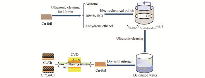
The Cu foil was carefully pretreated for 10 min each with acetone, 16wt% hydrochloric acid, and anhydrous ethanol to remove oxides and grease from the surface of copper foil. Electro-chemically polish the pretreated Cu foil for 15 min at 3.5 V to smooth the surface and reduce the nucleation sites, which helps to grow few layers of graphene. Then graphene was synthesized on Cu foil in CVD chamber by setting the response curve. With Cu foil in the space, the chamber was pumped down and the temperature ramped up 20 ℃/min with 60sccm argon (Ar) and 35sccm hydrogen (H2). Next, keep the temperature for 30 min with 60sccm Ar and 35sccm H2 for Cu foil annealing, which can increase the copper grain for growing graphene with large areas.
In the process of growing graphene, graphene of different layers grown with different gas ratios, growth time after introducing the carbon precursor (CH4). Then CH4 was turned off, and the CVD reactor began to cool with 500sccm Ar. Try to grow graphene on one side and two sides of Cu foil to make different layers graphene of Cu/Gr and Gr/Cu/Gr composite, as shown in Fig. 1. Place copper foil horizontally on a quartz boat with a quartz substrate below, and only the upper carbon source flows through copper foil to nucleate and grow graphene to prepare Gr/Cu composite. Copper foil is suspended and placed horizontally on a quartz boat, and carbon source air flows through both the upper and lower surfaces of copper foil to form graphene and prepare Gr/Cu/Gr composite. The Gr/Cu/Gr is prepared in one go by CVD, which enables saving the time and cost of preparation. Then different volume fraction and layers of graphene were used to evaluate their influence on the electrical conductivity of the Gr/Cu composites materials.
|
Fig.1 Fabrication process for Cu/Gr and Gr/Cu/Gr composites with sandwich type |
2 Results and Discussion 2.1 Characterization of Cu Foil After Polishing
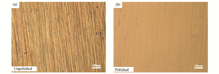
Optical microscopy (OM) of copper foil surface before and after electrochemical polishing are shown in Fig. 2. The step stripe on the surface of copper will deflect the crystal direction of graphene, which tends to form grain boundaries and other defects that is not conducive to the preparation of high-quality graphene. Therefore, electrochemical polishing of copper foil is required. The unpolished Cu foil shows large mechanical marks and impurity defects. After polishing, the flatness of the Cu foil surface is significantly enhanced, and the mechanical traces of the original copper foil are almost completely etched away to get smoother surface in Fig. 2(b). The smoother surface of Cu foil will help to reduce the nucleation sites of graphene, which is good for growing a few layers graphene with large area.
|
Fig.2 Optical microscope images of Cu foil |
2.2 Characterization of Graphene for Growth
In the first step of experiments, the smooth copper foil after pretreatment was heated up to 1035 ℃ in a controlled ambient (60sccm H2 and 35sccm Ar). Stabilize the chamber at 1035 ℃ for different time before introducing the carbon precursor (annealing step with 60sccm H2 and 20sccm Ar). During the annealing process, the recrystallization growth of Cu foil grains will increase their size. The larger grains are conducive to the growth of high coverage graphene and will reduce atomic scattering at grain boundaries, which helps to enhance the electrical conductivity of Cu foil[25-26].
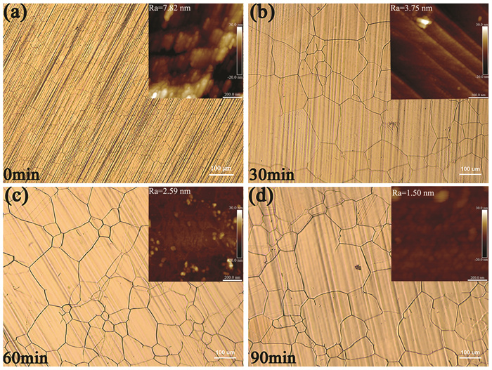
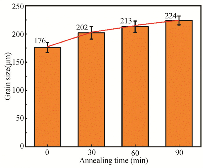
The appearance and grain size of Cu foil are observed by optical microscope, at different annealing time, as shown in Fig. 3. The surface of Cu foil is rough with blurred grain boundary for 0 min annealing time. When the annealing time is maintained for 30 min, the grain boundary is clear with increased grain size and the surface becomes flatter. Because the roughness of the Cu foil as determined by AFM at various annealing time is shown in the upper right corner of the OM diagram; as the annealing time increases, the roughness of the copper foil falls from 7.28 nm to 1.50 nm and the grain size of Cu foil increases. Five sets of OM photos are taken for each sample. According to the international standard YS/T347-2004, a line segment is drawn on the grain image as the measurement line segment. The magnification of 50 is selected to ensure that at least 50 grains are cut by line segments, and the average grain intercept is calculated. 15 groups of different grain sizes are obtained for different annealing time at 1035 ℃. After statistical processing of the data, the bar chart is obtained, as shown in Fig. 4. The average grain size increased by nearly 30 μm from 0 min to 30 min, but the grain size only increased by about 10 μm from 30 min to 60 min and 60 min to 90 min. After annealing for 30 min, the increase of grain size is not significant with the extension of annealing time. Considering the production cost and energy consumption of graphene, 30 min is the most cost-effective and appropriate annealing time.
|
Fig.3 Optical microscope images of Cu foil at different annealing time |
|
Fig.4 Copper grain size at different annealing time |
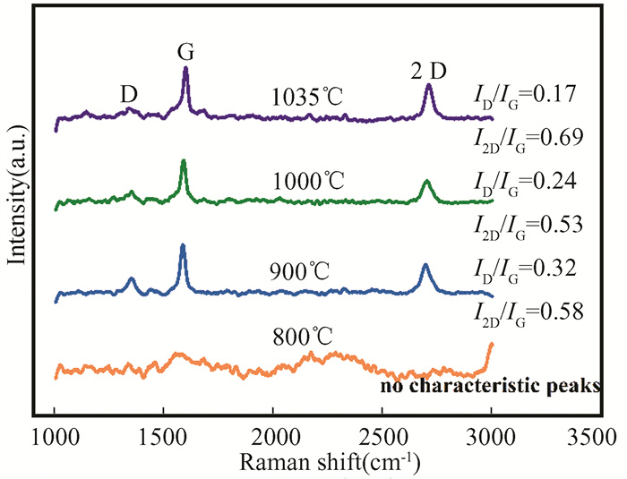
When the Cu foil was annealed for 30 min, the 20sccm CH4 was introduced to grow graphene with 15sccm H2 and 20sccm Ar. The nucleation and growth process of graphene is essentially the result of adsorption, desorption and migration of active carbon atoms, which are significantly affected by temperature. The growth temperature directly affects the nucleation and growth rate of graphene. Thus, the growth of graphene at different temperatures by CVD was analyzed by Raman characterization. Some typical Raman spectra of four temperatures from 800 ℃ to 1035 ℃ for synthesizing graphene were shown in Fig. 5. According to related studies, graphene cannot be generated by CVD at 800 ℃, and it can only be formed continuously at temperatures beyond 1000 ℃[27-28]. For this reason, we choose these four temperatures. And the growth time of graphene is 25 min. The D peak, G peak and 2D peak are the typical characteristic peaks of graphene. Peak D is only present when there are defects in graphene. The peak intensity ratio of the D and G bands (ID/IG) reflects the defects of graphene while the peak intensity ratio of 2D peak and G peak (I2D/IG) is connected with the number layers of graphene. No graphene forms at 800 ℃. At low temperature, the ability of graphene nucleus to capture carbon atoms is dominated by the nucleation density[29]. Therefore, the temperature of 800 ℃ is too low for graphene to be able to capture carbon atoms and form graphene.
|
Fig.5 Raman spectra of graphene grown at four different temperatures |
Liu et al.[30] believed that increasing temperature would reduce the roughness of the surface substrate, thereby reducing the nucleation activity sites and improving the mobility of the active material, which is inclined to grow uniform, continuous and low defective high-quality graphene. With increasing the growth temperature, the ID/IG ratio decreased, indicating that the graphene had fewer defects[31]. The ID/IG ratio for graphene growth at 1035 ℃ is the lowest, only less than 0.2, showing that 1035 ℃ is the relative optimum temperature for growth of graphene. Because the graphene grown at 1035 ℃ owns the best quality with few defects. The Raman spectra clearly shows that I2D/IG ratio is below 0.7, which is the ratio of multilayer graphene. Therefore, the optimum parameters for the growth of multilayer graphene (>2 layers) are obtained. The growth parameters of bilayer graphene and monolayer graphene are determined by the same method, as shown in Table 1. And the preparation of different layers graphene by CVD is in Fig. 6.
| Table 1 Parameters for the graphene growth |
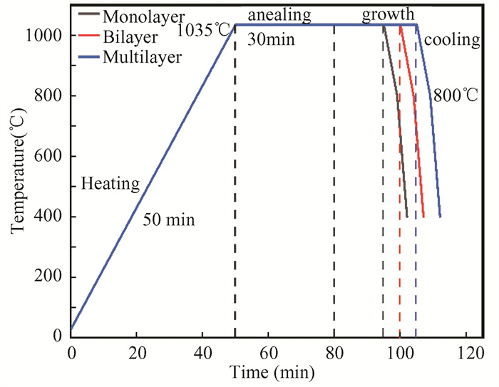
|
Fig.6 Schematic of different layers graphene |
The schematic of different layers graphene is shown in Fig. 6. For different layers graphene, the heating and annealing process are the same: the smooth copper foil was heated to 1035 ℃ in 60sccm H2 and 35sccm Ar flow (heating step) for 50 min at 200 Pa in the chamber. Then hold the 60sccm H2 and 20sccm Ar flow for 30 min (annealing step). Next, it is the growth of graphene. The temperature of 1035 ℃ was kept constant throughout the growth process. For monolayer graphene, keep 15sccm CH4, 20sccm H2 and 20sccm Ar at 1035 ℃ for 15 min; Bilayer graphene is grown with 20sccm CH4, 20sccm H2 and 20sccm Ar for 20 min; And the multilayer graphene is in the 20sccm CH4, 15sccm H2 and 20sccm Ar for 25 min. The temperature was then reduced to 800 ~C using a 500 sccm Ar flow. Finally, remove the furnace away from the sample holding area and allow the chamber to cool further to room temperature.
The conductivity of graphene depends on the size, number of layers and defect density. Next, we did investigate the effect of the layers(n) of graphene embedded in the copper matrix on the conductivity. The grown graphene films with different number of layers were characterized by Raman, as shown in Fig. 7. By carefully controlling the CH4 concentration and graphene growth time by CVD, monolayer, bilayer and multilayer graphene were deposited on Cu.

|
Fig.7 Raman characterization of graphene with different layers |
Fig. 8 and Fig. 9 show the Raman contour plots of graphene, which are related to the structural integrity and uniformity of the deposited graphene. Different ratio of I2D/IG represents the layers of graphene. It is generally believed that the monolayer nature of graphene's I2D/IG is over 1.4; an I2D/IG ratio of 0.7-1.4 indicates the bilayer nature of graphene; and multilayer graphene owns the ratio of I2D/IG less than 0.7. In the Raman spectra of graphene, the intensity ratio of I2D/IG is associated with the number of graphene layers, corresponding to the different colors in Fig. 8. The result of Fig. 8 is tested in a random with an area of 50 × 50 μm2, which shows that monolayer, bilayer and multilayer graphene's coverage. For monolayer, more than 90% ratio of I2D/IG is over 1.4, indicating that the monolayer graphene covers up to 90%, indicating that the graphene occupies approximately 21 cm2 on the copper foil. While as for the Raman contour plots of bilayer graphene, the coverage of I2D/IG ratio range 0.7 to 1.4 is 70%-80%. And the multilayer graphene*s coverage is 80%. The coverage of a certain layer of graphene is less than 100%, because there are some different layers of graphene that appeared during the CVD process while preparing a certain number of layers of graphene. This is due to the unavoidable inhomogeneities in the CVD coating process. However, the graphene prepared has high coverage, especially the monolayer graphene covering up to 90%, indicating that the grown graphene was continuous and uniform.
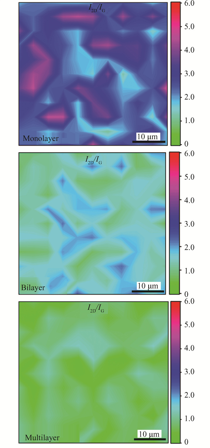
|
Fig.8 Raman contour plots of the intensity ratio of the 2D peak to the G peak(I2D/IG) |
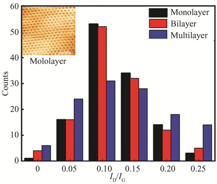
|
Fig.9 Histogram statistical graph of ID/IG in Raman spectra |
The ratio of the ID/IG is positively correlated with defects in graphene[32]. The defect density is calculated with an area of 50 × 50 μm2 (Fig. 9) and counting the defects of different layer graphene within the area. The prepared graphene*s ratio of ID/IG is all below 0.25 and mainly between 0.1 and 0.15, indicating the high quality of the growth graphene. Compared with multilayer graphene, the monolayer and bilayer graphene ratio of ID/IG is mainly concentrated in 0.05 and 0.2 with smaller defects, which presents that few layers of graphene are easier to obtain high quality. At the same time, the prepared monolayer graphene was characterized by scanning tunneling microscope (STM), as shown in the upper left corner of Fig. 9. The results showed that the honeycomb graphene was uniformly shaped, indicating that the graphene prepared was of high quality and continuous uniformity. The Raman spectra results (Fig. 8 and Fig. 9) illustrate high-quality graphene with uniform and high coverage was grown on Cu foil.
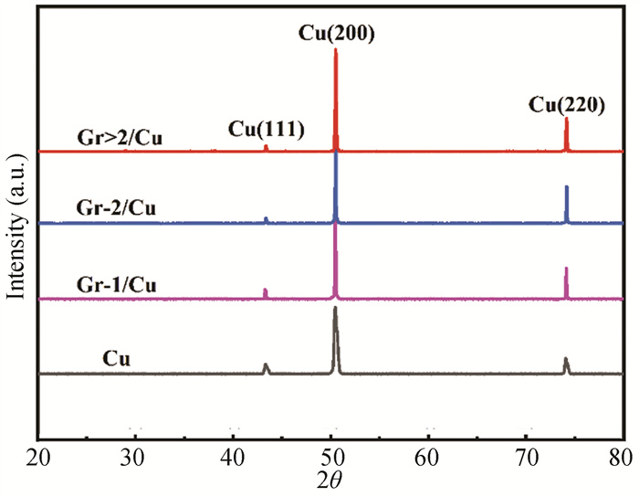
Fig. 10 shows the X-ray diffraction pattern (XRD) patterns of different graphene layers of Gr/Cu composite. Among them, Gr-1, Gr-2, Gr>2 stand for monolayer graphene, bilayer graphene and multilayer graphene, respectively. It is clearly detected three characteristic peaks of Cu with different layers graphene Gr/Cu composite in the XRD spectrum. In the XRD patterns, the indices of Cu (111), Cu (200) and Cu (220) can be seen without Cu oxide diffraction peak in the graphene/copper composite, indicating that no or only slight oxidation occurs during the preparation of the graphene on the Cu foil. Compared with pure Cu, the diffraction peak width of Gr/Cu composite decreased, which implied that the Cu foil was recrystallized to improve grain size while growing the graphene by using CVD. There is no carbon diffraction peak, which is probably due to the relatively small content of graphene. Therefore, the graphene is not detected by XRD.
|
Fig.10 XRD patterns of different Gr layers of Gr/Cu composite |
The structural integrity and homogeneity of the deposited graphene were shown in Fig. 11. The growth graphene appears transparent and smooth wrinkled and the wrinkled graphene can grow continuously across grain boundaries on copper foil, which helps electrons travel along the graphene at grain boundaries, reducing the effect of grain boundary scattering on electron transport. The wrinkles result from a mismatch between the coefficients of thermal expansion graphene and the underlying Cu foil[33]. Fig. 11(b) and (c) show the SEM and TEM of graphene with some wrinkles that are stripped from the Gr/Cu composite material by etching away the Cu foil. A layer of PMMA was spun on the surface of Gr/Cu composite material to protect graphene, forming PMMA/Gr/Cu composite which was etched in FeCl3 at 45℃ for 6 h. After the copper foil was entirely dissolved, the Gr/PMMA layer was cleaned and transferred to the silicon wafer. Then dissolving PMMA in acetone at 60 ℃ for 30 min to get graphene. The stripped graphene was of a nearly transparent lamellar structure and crimped at the edges. And the graphene owns a large and continuous area, indicating the graphene is uniformly coated on the copper foil.

|
Fig.11 Characterization of microstructure of Gr/Cu composite material |
2.3 Electrical Conductivity Properties
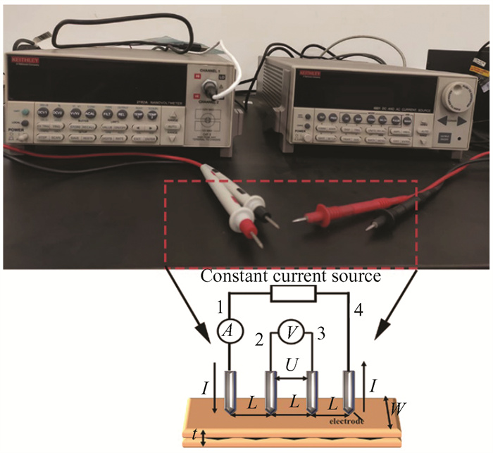
In regard to the electrical conductivity of the Gr/Cu composites, the Keithley 2182A/6221 system with Delta Mode combined four-point method was utilized to describe the electrical conductivity in order to remove the thermal resistance, contact resistance and measurement error, as shown in Fig. 12. The resistivity of Cu/Gr composite was calculated using the following equation:
|
Fig.12 Schematic diagram of resistance test for composite materials |
| $ \rho=d \cdot R_s $ | (1) |
| $ \sigma=\frac{1}{\rho} $ | (2) |
where ρ is resistivity, d is the thickness, Rs is the square resistance and σ is the conductivity.
As shown in Fig. 13, the conductivity of Gr/Cu and Gr/Cu/Gr decreased as the number of graphene layers increased. The thickness of monolayer graphene is 0.35 nm, and the thickness of graphene increases by multiple times as the number of graphene layers increases. The conductivity of Gr/Cu/Gr was higher than Gr/Cu due to the increased content of graphene. The Gr/Cu/Gr with monolayer has the optimal electrical conductivity compared with bilayer and multilayer graphene of Gr/Cu/Gr composite. Because the lattice structure of single-layer graphene is simpler, there is no interface effect caused by layering to reduce the conductivity of the graphene. The conductivity of Gr/Cu and Gr/Cu/Gr coated with monolayer graphene are 58.2×10⁶ and 59.8×10⁶ S/m. Compared with pure Cu and annealed Cu, the conductivity of Gr/Cu and Gr/Cu/Gr is significantly improved, as shown in Fig. 14.

|
Fig.13 Electrical conductivity of different layers Gr/Cu composite |

|
Fig.14 Electrical conductivity of monolayer graphene of Gr/Cu composite |
Considering that the thickness of polished Cu foil is 45 μm and monolayer graphene is ~0.35 nm, the relative volume fraction of graphene is ~0.002vol%. The conductivity of Gr/Cu is 1.75% higher than annealed copper (57.2×10⁶ S/m). The Gr/Cu/Gr composite is about 4.5% higher than annealed Cu and 5.3% higher than pure Cu, which is equivalent to 104.5% IACS.
2.4 DiscussionWhile many studies have been carried out to make graphene-copper composites for enhancing the property of Cu. However, most of them improved the mechanical performance of Cu matrix while also reducing the electrical conductivity. Therefore, how to better use the superior electrical properties of graphene in Cu composites to improve the electrical conductivity of Cu is still a great challenge. Compared with previous studies, the work completed here has prepared monolayer, bilayer and multilayer graphene with high quality over a large area by CVD, leading to intimate contact between the fabricated graphene and the Cu foil.
The Gr/Cu and Gr/Cu/Gr composite was fabricated with monolayer graphene, bilayer graphene and multilayer graphene. The electrical conductivity of Gr/Cu and Gr/Cu/Gr decreased with the increasing layer numbers of graphene. And by stacking graphene on the Gr/Cu to form sandwich-type Gr/Cu/Gr, the electrical conductivity of graphene/copper composite has been increased, mainly due to the combination of the high free electron density of metallic Cu and the long mean free path of graphene. During the process of graphene grown by CVD, the graphene got homogenous distribution and good interface combination with Cu foil, which helped to improve electrical conductivity of pure Cu. Meanwhile, The transboundary growth of graphene on copper foil enabled electrons to be transported by graphene instead of grain boundary, which reduced the scattering effect of grain boundaries on conduction electrons. So the graphene growth on the Cu foil improved the conductivity of pure copper.
Therefore, the sandwich-type monolayer-Gr/Cu/monolayer-Gr has most enhanced the best electrical conductivity of Cu with only ~0.002% volume fraction of graphene, and the conductivity of the composite is improved to 104.5%IACS and 105.3% pure Cu. By comparing the electrical conductivity of this work vs. the reported studies on graphene/copper composites, it is obvious to conclude that improving the interface bonding and the quality of graphene is promising to improve the electrical conductivity of graphene/copper composites. Meanwhile, the high electrical conductivity and little graphene volume fraction of monolayer graphene of Gr/Cu/Gr make the composite outstanding among graphene/copper composites prepared using different methods to form various Cu matrix composites, as shown in Fig. 15[10, 18, 20, 22, 34-36].

|
Fig.15 Comparision of electrical conductivity of Gr/Cu composites with other copper-carbon composites |
Although, the integration of graphene is able to increase the mechanical and electrical properties, the volume fraction is too small (~0.002vol%). An extremely low graphene content is required to attain ultra-high conductivity. The result shows that the specific enhancement effect of graphene on the conductivity of Cu could be better if appropriate Gr/Cu composite can be developed.
3 ConclusionsHigh quality monolayer, bilayer and multilayer graphene are obtained by carefully controlling the time, temperature and the gas ratio during the CVD process. The defect of graphene received is most less than 0.2 and the graphene uniformly covers the Cu foil with about 90% coverage, and the graphene/copper composites with different layers of graphene are successfully fabricated and the resultant conductivities are tested.
Both Gr/Cu and Gr/Cu/Gr composites are fabricated by using CVD method with adjusted parameters. Results have shown that the conductivity of the sandwich type Gr/Cu composite increases with the increase of graphene volume fraction and the decrease of graphene layers. The Gr/Cu/Gr composite with monolayer owns the best conductivity with ~0.002vol% graphene, up to 59.8×10⁶ S/m, which is equivalent to 104.5% IACS and 105.3% pure Cu foil, achieving ultra-high conductivity. Thus, the graphene volume fraction (1%) can increase the conductivity of Cu by 26.5 times if the volume fraction of monolayer graphene in the sandwiched type is appropriately increased. These results can be used to guide further development of Gr/Cu composites to meet application needs.
AcknowledgementThis work was supported substantially by the Southwest Jiaotong University for Material and Financial Support. And the authors would like to thank Ceshigo Research Service for some supports to SEM and TEM tests.
| [1] |
Qu W, Zhang J, Zhang S, et al. Copper matrix composites reinforced by three-dimensional netlike graphene towards enhanced mechanical property and wear resistance. Composites Communications, 2022, 32: 101187. DOI:10.1016/j.coco.2022.101187 (  0) 0) |
| [2] |
Lin Z D, Shu S C, Li A, et al. Preparation and mechanical property of graphene-reinforced copper matrix composites. Journal of Inorganic Materials, 2019, 34(5): 469-477. DOI:10.15541/jim20180393 (  0) 0) |
| [3] |
Stoller M D, Park S, Zhu Y, et al. Graphene-based ultracapacitors. Nano Letters, 2008, 8(10): 3498-3502. DOI:10.1021/nl802558y (  0) 0) |
| [4] |
Castro Neto A H, Guinea F, Peres N M R, et al. The electronic properties of graphene. Review of Modern Physics, 2009, 81(1): 109-162. DOI:10.1103/RevModPhys.81.109 (  0) 0) |
| [5] |
Choi W, Lahiri I, Seelaboyina R, et al. Synthesis of graphene and its applications: a review. Critical Reviews in Solid State and Materials Sciences, 2010, 35(1): 52-71. DOI:10.1080/10408430903505036 (  0) 0) |
| [6] |
Park J, Yan M. Covalent functionalization of graphene with reactive intermediates. Accounts of Chemical Research, 2013, 46(1): 181-189. DOI:10.1021/ar300172h (  0) 0) |
| [7] |
Chen J H, Jang C, Xiao S, et al. Intrinsic and extrinsic performance limits of graphene devices on SiO2. Nature Nanotech, 2008, 3(4): 206-209. DOI:10.1038/nnano.2008.58 (  0) 0) |
| [8] |
Balandin A A, Ghosh S, Bao W, et al. Superior thermal conductivity of single-layer graphene. Nano Letters, 2008, 8(3): 902-907. DOI:10.1021/nl0731872 (  0) 0) |
| [9] |
Zhang F, Wang J, Liu T, et al. Enhanced mechanical properties of few-layer graphene reinforced titanium alloy matrix nanocomposites with a network architecture. Materials & Design, 2020, 186: 108330. DOI:10.1016/j.matdes.2019.108330 (  0) 0) |
| [10] |
Nazeer F, Ma Z, Gao L, et al. Thermal and mechanical properties of copper-graphite and copper-reduced graphene oxide composites. Composites Part B: Engineering, 2019, 163: 77-85. DOI:10.1016/j.compositesb.2018.11.004 (  0) 0) |
| [11] |
Shao G, Liu P, Li W, et al. Effects of graphene nanoplates on arc erosion resistance and wear behavior under electric current of copper matrix composites. Journal of Alloys and Compounds, 2020, 829: 154356. DOI:10.1016/j.jallcom.2020.154356 (  0) 0) |
| [12] |
Jiang R, Zhou X, Liu Z. Electroless Ni-plated graphene for tensile strength enhancement of copper. Materials Science and Engineering: A, 2017, 679: 323-328. DOI:10.1016/j.msea.2016.10.029 (  0) 0) |
| [13] |
Tang Y, Yang X, Wang R, et al. Enhancement of the mechanical properties of graphene-copper composites with graphene-nickel hybrids. Materials Science and Engineering: A, 2014, 599: 247-254. DOI:10.1016/j.msea.2014.01.061 (  0) 0) |
| [14] |
Yue H, Yao L, Gao X, et al. Effect of ball-milling and graphene contents on the mechanical properties and fracture mechanisms of graphene nanosheets reinforced copper matrix composites. Journal of Alloys and Compound, 2017, 691: 755-762. DOI:10.1016/j.jallcom.2016.08.303 (  0) 0) |
| [15] |
Song G, Wang Q, Sun L, et al. One-step synthesis of sandwich-type Cu/Graphene/Cu ultrathin foil with enhanced property via electrochemical route. Materials & Design, 2020, 191: 108629. DOI:10.1016/j.matdes.2020.108629 (  0) 0) |
| [16] |
Cao M, Xiong D, Yang L, et al. Ultrahigh electrical conductivity of graphene embedded in metals. Advanced Functional Materials, 2019, 29(17): 1806792. DOI:10.1002/adfm.201806792 (  0) 0) |
| [17] |
Dong Z, Peng Y, Tan Z, et al. Simultaneously enhanced electrical conductivity and strength in Cu/Graphene/Cu sandwiched nanofilm. Scripta Materialia, 2020, 187: 296-300. DOI:10.1016/j.scriptamat.2020.06.051 (  0) 0) |
| [18] |
Cao M, Xiong D B, Tan Z, et al. Aligning graphene in bulk copper: nacre-inspired nanolaminated architecture coupled with in-situ processing for enhanced mechanical properties and high electrical conductivity. Carbon, 2017, 117: 65-74. DOI:10.1016/j.carbon.2017.02.089 (  0) 0) |
| [19] |
Novoselov K S, Geim A K, Morozov S V, et al. Electric field effect in atomically thin carbon films. Science, 2004, 306(5696): 666-669. DOI:10.1126/science.1102896 (  0) 0) |
| [20] |
Yang M, Weng L, Zhu H, et al. Simultaneously enhancing the strength, ductility and conductivity of copper matrix composites with graphene nanoribbons. Carbon, 2017, 118: 250-260. DOI:10.1016/j.carbon.2017.03.055 (  0) 0) |
| [21] |
Chen F, Ying J, Wang Y, et al. Effects of graphene content on the microstructure and properties of copper matrix composites. Carbon, 2016, 96: 836-842. DOI:10.1016/j.carbon.2015.10.023 (  0) 0) |
| [22] |
Yao G C, Mei Q S, Li J Y, et al. Cu/C composites with a good combination of hardness and electrical conductivity fabricated from Cu and graphite by accumulative roll-bonding. Materials & Design, 2016, 110: 124-129. DOI:10.1016/j.matdes.2016.07.129 (  0) 0) |
| [23] |
Li X, Colombo L, Ruoff R S. Synthesis of graphene films on copper foils by chemical vapor deposition. Advanced Materials, 2016, 28(29): 6247-6252. DOI:10.1002/adma.201504760 (  0) 0) |
| [24] |
Chaitoglou S, Amade R, Bertran E. Insights into the inherent properties of vertical graphene flakes towards hydrogen evolution reaction. Applied Surface Science, 2022, 592: 153327. DOI:10.1016/j.apsusc.2022.153327 (  0) 0) |
| [25] |
Wang H, Wang G, Bao P, et al. Controllable synthesis of submillimeter single-crystal monolayer graphene domains on copper foils by suppressing nucleation. Journal of the American Chemical Society, 2012, 134(8): 3627-3630. DOI:10.1021/ja2105976 (  0) 0) |
| [26] |
Li X, Cai W, An J, et al. 25-large-area synthesis of high-quality and uniform graphene films on copper foils. Science, 2009, 324(5932): 1312-1314. DOI:10.1126/science.1171245 (  0) 0) |
| [27] |
Bertran S E, Musheghyan A A, Chaitoglou S, et al. Temperature-modulated synthesis of vertically oriented atomic bilayer graphene nanowalls grown on stainless steel by inductively coupled plasma chemical vapour deposition. Applied Surface Science, 2023, 610: 155530. DOI:10.1016/j.apsusc.2022.155530 (  0) 0) |
| [28] |
Chaitoglou S, Bertran E. Effect of temperature on graphene grown by chemical vapor deposition. Journal of Materials Science, 2017, 52(13): 8348-8356. DOI:10.1007/s10853-017-1054-1 (  0) 0) |
| [29] |
Kim H, Mattevi C, Calvo M R, et al. Activation energy paths for graphene nucleation and growth on Cu. ACS Nano, 2012, 6(4): 3614-3623. DOI:10.1021/nn3008965 (  0) 0) |
| [30] |
Liu L, Zhou H, Cheng R, et al. A systematic study of atmospheric pressure chemical vapor deposition growth of large-area monolayer graphene. Journal of Materials Chemistry, 2012, 22(4): 1498-1503. DOI:10.1039/C1JM14272K (  0) 0) |
| [31] |
Hu B, Ago H, Ito Y, et al. Epitaxial growth of large-area single-layer graphene over Cu (111)/sapphire by atmospheric pressure CVD. Carbon, 2012, 50(1): 57-65. DOI:10.1016/j.carbon.2011.08.002 (  0) 0) |
| [32] |
Ferrari A C, Meyer J C, Scardaci V, et al. Raman spectrum of graphene and graphene layers. Physical Review Letters, 2006, 97(18): 187401. DOI:10.1103/PhysRevLett.97.187401 (  0) 0) |
| [33] |
Regmi M, Chisholm M F, Eres G. The effect of growth parameters on the intrinsic properties of large-area single layer graphene grown by chemical vapor deposition on Cu. Carbon, 2012, 50(1): 134-141. DOI:10.1016/j.carbon.2011.07.063 (  0) 0) |
| [34] |
Yang T, Chen W, Zhang H, et al. In-situ generated graphene from wheat flour for enhancing mechanical and electrical properties of copper matrix composites. Materials Science and Engineering: A, 2022, 835: 142662. DOI:10.1016/j.msea.2022.142662 (  0) 0) |
| [35] |
Zhang X, Xu Y, Wang M, et al. A Powder-metallurgy-based strategy toward three-dimensional graphene-like network for reinforcing copper matrix composites. Nature Communications, 2020, 11(1): 2775. DOI:10.1038/s41467-020-16490-4 (  0) 0) |
| [36] |
Luo H, Sui Y, Qi J, et al. Mechanical enhancement of copper matrix composites with homogeneously dispersed graphene modified by silver nanoparticles. Journal of Alloys and Compounds, 2017, 729: 293-302. DOI:10.1016/j.jallcom.2017.09.102 (  0) 0) |
 2024, Vol. 31


